8096 Microcontroller Architecture Block Diagram:
Fig. 13.1 shows the internal block diagram of 8096 Microcontroller Architecture Block Diagram. It consists of several functional units, namely
- CPU with 232 byte register file and register ALU
- 8-Kbyte internal ROM
- Programmable high speed I/O unit.
- Two 16-bit Timers/Counters
- Serial port
- Pulse width modulator
- Watchdog timer
- Eight multiplexed inputs analog to digital converter with 10 bit resolution and
- Memory controller
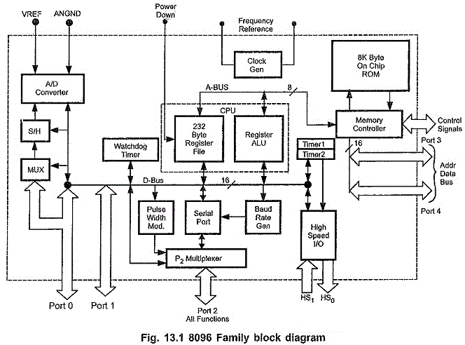
In addition to these functional units, there are some sections which support overall operation of the chip such as the clock generator and baud rate generator.
Two mainbuses (A-bus and D-bus) are used for inter-processor communication. A-bus is a 8-bit address bus and D-bus is a 16-bit data bus. The D-bus transfers data only between the RALU and the register file or special function registers (SFRs).
The A-bus provides the addresses for above transfers or address for multiplexed address/data bus connecting to the memory controller. The memory controller provides the addresses for the internal ROM and external memory.
The 8096 Microcontroller Architecture Block Diagram functional units can be divided into two major sections :
- CPU section and
- I/O section.