Intel 8051 Architecture and 8031 Architecture:
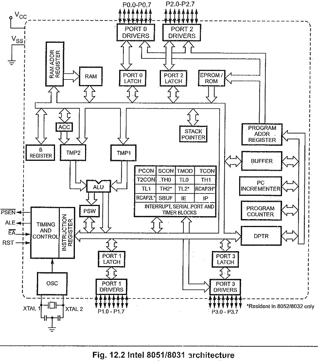
Fig. 12.2 shows the Intel 8051 Architecture and 8031 Architecture. It consists of a Central Processing Unit, two kinds of memory (data RAM plus program ROM/EPROM) Input/Output ports, the mode status, and data registers and random logic needed for a variety of peripheral functions. These elements communicate through an eight bit data bus which runs throughout the chip referred as internal data bus. This bus is buffered to the outside world through an I/O port when memory or I/O expansion is desired.
Central Processing Unit (CPU):
The CPU of 8051 Architecture consists of eight-bit Arithmetic and Logic unit with associated registers like A, B, PSW, SP, the sixteen bit program counter and “Data pointer” (DPTR) registers.
ALU:
The 8051’s ALU can perform arithmetic and logic functions on eight bit variables. The arithmetic unit can perform addition, subtraction, multiplication and division. The logic unit can perform logical operations such as AND, OR, and Exclusive-OR, as well as rotate, clear, and complement. The ALU also looks after the branching ‘decisions. An important and unique feature of the Intel 8051 Architecture and 8031 Architecture is that the ALU can also manipulate one bit as well as eight-bit data types. Individual bits may be set, cleared, complemented, moved, tested, and used in logic computation.
Accumulator:
It is an 8-bit register. It holds a source operand and receives the result of the arithmetic instructions (addition, subtraction, multiplication, and division). The accumulator can be the source or destination for logical operations and a number of special data movement instructions, including look-up tables and external RAM expansion. Several functions apply exclusively to the accumulator : rotate, parity computation, testing for zero, and so on.
In addition to accumulator, an 8-bit B-register is available as a general purpose register when it is not being used for the hardware multiply/divide operation.
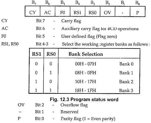
Program Status Word:
Many instructions implicitly or explicitly affect (or are affected by) several status flags, which are grouped together to form the Program Status Word. Fig. 12.3 shows the bit pattern of the program status word. It is an 8-bit word, containing the information as follows.
Other CPU Registers:
Stack Pointer :
The stack pointer register is 8 bit wide. It is incremented before data is stored during PUSH and ALL instructions. The stack array can reside anywhere in on-chip RAM. The stack pointer is initialized to 07H after a reset. This causes the stack to begin at location 08H.
Data Pointer (DPTR) :
The data pointer (DPTR) consists of a high byte (DPH) and a low byte (DPL). Its function is to hold a 16 bit address. It may be manipulated as a 16 bit data register or as two independent 8 bit registers. It serves as a base register in indirect jumps, lookup table instructions and external data transfer.
Memory Structure of 8051:
Fig: 12.4 shows the basic memory structure for 8051. It can access upto 64 K program memory and 64 K data memory. The 8051 has 4 Kbytes of internal program memory and 256 bytes of internal data memory.
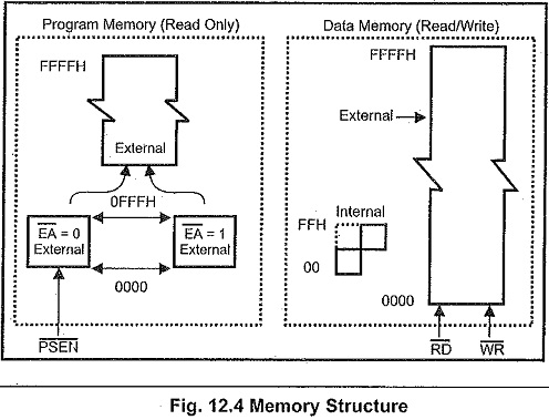
Each memory type has different addressing mechanism, different control signals, and a differennt function. Each may be added independently, and each uses the same address and data buses, but with different control signals.
Program Memory of 8051 :
Fig. 12.5 shows a map of Program Memory of 8051.
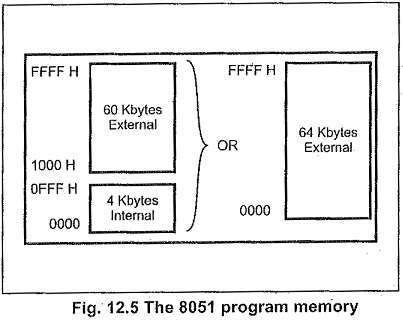
In 8051, when the EA pin is connected to Vcc, program fetches to addresses 0000H through OFFFH are directed to the internal ROM and program fetches to addresses 1000H through FFFFH are directed to external ROM/EPROM. On the other hand when EA pin is grounded, all addresses (0000H to FFFFH) fetched by program are directed to the external ROM/EPROM. The PSEN signal is used to activate output enable signal of the external ROM/EPROM , as shown in the Fig. 12.6.
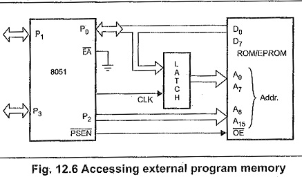
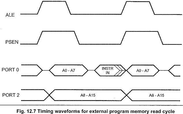
As shown in the Fig. 12.6, the port 0 is used as a multiplexed address/data bus. It gives lower order 8-bit address in the initial T-cycle and later it is used as a data bus.The 8-bit address is latched using external latch and ALE signal generated by Intel 8051 Architecture and 8031 Architecture. The port 2 provides the higher order 8-bit address. Fig. 12.7 shows the timing waveforms for external program memory read cycle.
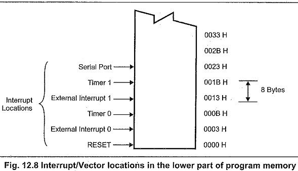
The lower part of program memory stores the vector addresses for various interrupt service routines. Fig. 12.8 shows the vector address map. Each interrupt is assigned with a fixed location in program memory. For example, external interrupt 0 is assigned to location 0003H. The interrupt service locations are spaced at 8-byte intervals such as 0003H for External Interrupt 0, 000BH for Timer 0, 0013H for External Interrupt 1, 001BH for Timer1, etc. If interrupt is going to be used, its service routine must begin at corresponding location. If the interrupt is not going to be used, its service location is available as general purpose program memory.
Memory Organisation of 8051:
Fig. 12.9 shows a map of Data Memory Organisation of 8051
The 8051 can address upto 64 Kbytes of external data memory. The “MOVX” instruction is used to access the external data memory. The internal data memory space for Intel 8051 Architecture and 8031 Architecture is divided into three blocks : Lower 128 bytes, Upper 128 bytes and SFRs. The upper addresses and SFRs occupy the same block of address space, 80H through FFH, although they are physically separate entities. As shown in the Fig. 12.9, the upper address space is accessible by indirect addressing only and SFRs are accessible by direct addressing only. On the other hand, lower address space can be accessed either by direct addressing or by indirect addressing.
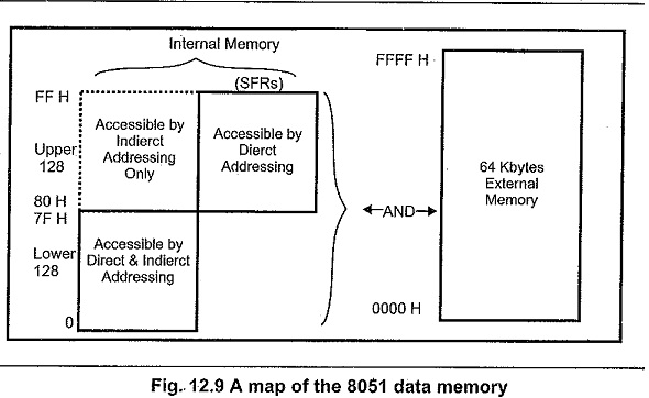
Fig. 12.10 shows the circuit diagram for connecting external data memory. The multiplexed address/data bus provided by port 0 is demultiplexed by external latch and ALE signal. Port 2 gives the higher order address bus. The RD and WR signals from 8051 selects the memory read and memory write operation, respectively.
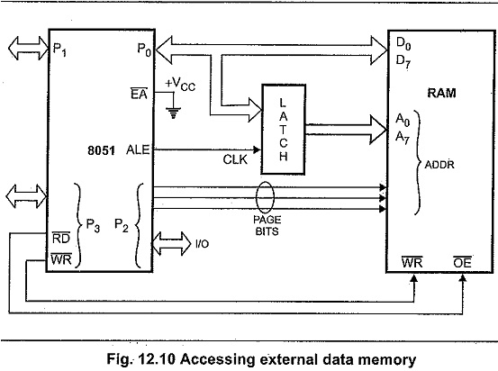
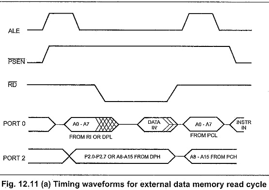
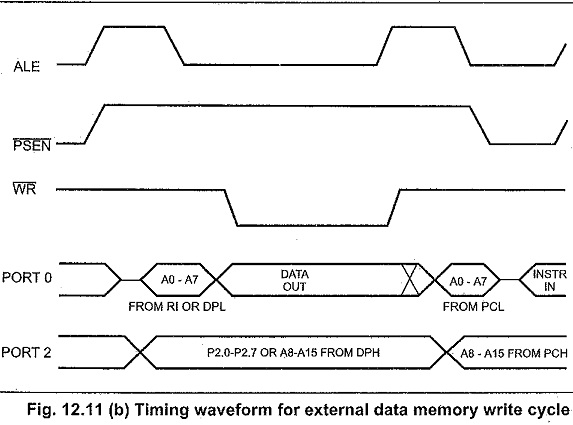
Fig. 12.11 (a) and (b) show the timing waveforms for external data memory read and write cycles, respectively.
In addition to the program and data memory, there is another physical address space, some of these – B, SP, PSW, DPH and DPL registers are discussed earlier. Others-I/O ports and peripheral function registers collectively referred as special function registers will be introduced in the following sections.
Special Function Register:
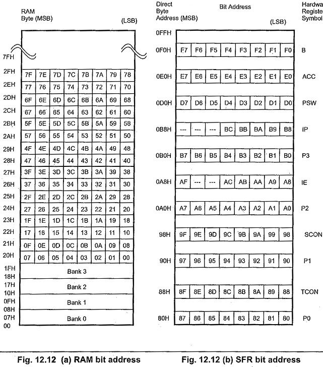
Unlike other microprocessors in the Intel family, 8051 uses memory mapped I/O through a set of special function registers that are implemented in the address space immediately above the 128 bytes of RAM. Fig. 12.12 shows special function bit addresses. All access to the four I/O ports, the CPU registers, interrupt-control registers, the timer/counter, UART, and power control are performed through registers between 80H and FFH.
RAM:
It consists of 4 register banks and 144 general purpose bits forming boolean processor RAM. Fig. 12.12 shows RAM bit addresses. The register bank-select bits refer to four 8 byte regions at the bottom of memory. Certain instructions can access these registers in RAM directly with 1 byte instructions, since 3 bits of the instruction specify the desired register. The RSO and RS1 bits in PSW must be set to the appropriate bank before execution of the instruction. This method of addressing saves one byte per instruction. The 144 general purpose bits can be used as software flags or program variables.
Input/Output Ports:
The MCS-51 family I/O port structure is extremely versatile. The 8051 has 32 I/0 pins configured as four eight-bit parallel ports ( P0, P1, P2, and P3 ). All four ports are bidirectional, i.e. each pin will be configured as input or output (or both) under software control. Each port consists of a latch, an output driver, and an input buffer.
The output drives of Ports 0 and 2 and the input buffers of Port 0, are used in access to external memory. As mentioned earlier, Port 0 outputs the low order byte of the external memory address, time multiplexed with the data being written or read, and Port 2 outputs the high order byte of the external memory address when the address is 16 bits wide. Otherwise Port 2 gives the contents of special function register P2.
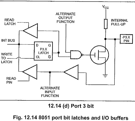
All port pins of Port 3 are multi functional. They have special functions as shown in Fig. 12.13 including two external interrupts, two counter inputs, two special data lines and two timing control strobes.
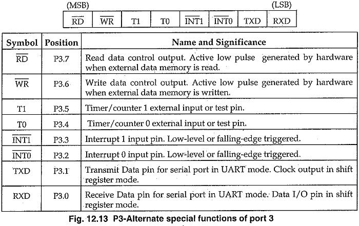
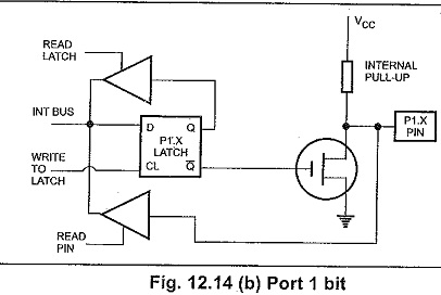
Fig. 12.14 shows a functional diagram of a typical bit latch and I/O buffers in each of the four ports. The bit latch is nothing but the one bit in the port’s SFR. It is represented as a D flip-flop. The signal “write to latch” acts as clock input for D flip-flop. The data from the internal bus is clock-in in response to a “write to latch” signal from the CPU. The Q output or Q output after inversion from D flip-flop is connected at the gate input of the drive FET. The On and OFF state of the drive FET due to the data available at the output of latch decides the status of the output pin. It is possible to read Q output of latch by activating “read latch” signal from the CPU. The actual port status can be read by activating “read pin” signal, as shown in Fig. 12.14.
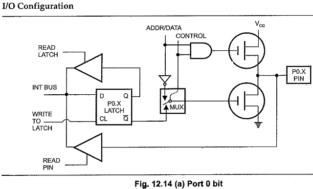
As.shown in the Fig. 12.14, for Port 0 and Port 2 drivers are switchable to internal ADDR/DATA and ADDR bus, respectively, by internal CONTROL signal. The switching is required to access external memory. During external memory acceses, the P2 SFR remains unchanged, but P0 SFR gets is written to it.
As mentioned earlier, Port 3 has multifunction pins. Therefore, each pin of Port 3 can be programmed to use as I/O or as one of the alternate function. This is achieved by the another control input, “Alternate output function’, as shown in the Fig. 12.14. When latch bit of Port 3 contains 1, the output level is controlled by control input, “alternate output function.”
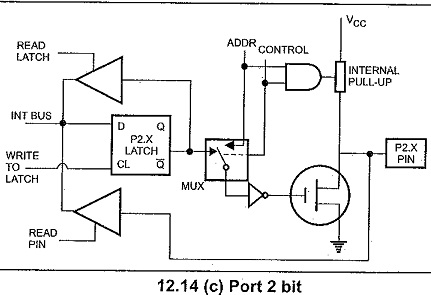
The port pin can be configured as an input by writing 1 in the latch bit of the corresponding pin. It turn OFF the output driver FET. Then for, Ports 1,2 and 3, the pin is pulled high by the internal pull-up, but can be pulled low by an external source. There is no internal pull-up for port 0. Therefore, its output pin floats when 1 is written in the latch bit, and pin can be used as a high impedance input. The port .0 is said to be “true bidirectional“, because when configured as an input it floats.
On the otherhand, the output of Ports 1,2 and 3 are pulled high with pull-up registers, when configured as an input. Thus they are sometimes called “quasi bidirectional” ports..
Special Peripheral Functions:
There are few common needs that microcomputer system should provide :
- Keeping track of elasped real-time.
- Maintaining a count of signal transitions
- Measuring the precise width of input pulses.
- Communicating with other systems or people.
- Closely monitoring asynchronous external events
Until now, microprocessor systems needed peripheral chips such as timers / counters, USARTs, or interrupt controllers to meet these needs. The Intel 8051 Architecture and 8031 Architecture family integrates all these capabilities on-chip.