Architecture of Pentium 4 Processor:
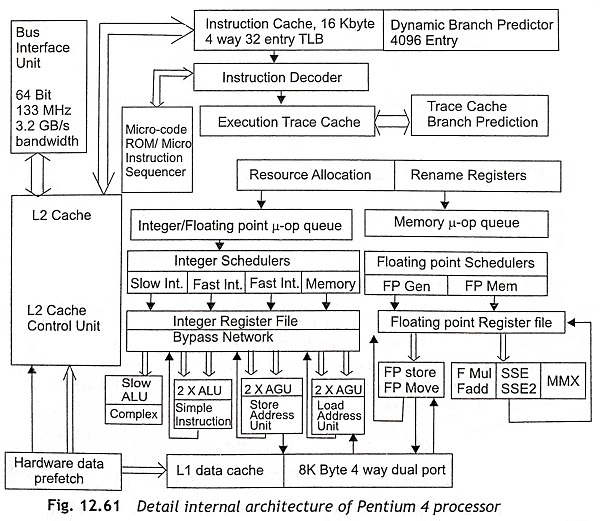
The simplified block diagram of internal architecture of Pentium 4 Processor is shown in Fig. 12.60 and the detailed internal architecture of Pentium 4 is depicted in Fig. 12.61. Generally, the Architecture of Pentium 4 Processor consists of a Bus Interface Unit (BIU), Instruction Fetch and Decoder Unit, Trace Cache (TC), Microcode ROM, Branch Target Buffer (BTB), Branch Prediction, Instruction Translation Look-aside Buffer (ITLB), Execution Unit, and Rapid Execution Module. It is clear from Fig. 12.60 that The Architecture of Pentium 4 Processor has four different modules such as (i) memory subsystem module, (ii) front-end module, (iii) integer/floating point execution unit, and (iv) out-of-order execution unit. The memory subsystem module contains a Bus Interface Unit (BIU) and L3 cache (optional). The front-end module consists of instruction decoder, Trace Cache (TC), microcode ROM, Branch Target Buffer (BTB) and branch prediction. Integer/Floating point execution unit has the L1 data cache and execution unit. The out-of-order execution unit consists of execution unit and retirement. In this section, the detailed internal Architecture of Pentium 4 Processor has been discussed elaborately.
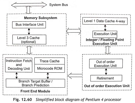
Bus interface Unit (BIU) The Bus Interface Unit (BM) is used to communicate with the system bus, cache bus, L2 cache, L1 data cache and L1 code cache.
Instruction Decoder The instruction decoder is used to decode all instructions of the Pentium 4 processor concurrently and translate them into micro-operations (μ-ops). One instruction decoder decodes one instruction per clock cycle. Simple instructions are translated into one μ-ops, but other instructions are translated into multiple numbers of μ-ops. Usually, a complex instruction requires more than four μ-ops. Therefore, the decoder cannot decode complex instructions and it transfers the task to a Microcode ROM.
Trace Cache (TC) After translation of instructions into micro-operations (μ-ops) by using an instruction decoder, the streams of decoded instructions are fed to an L1 instruction cache, which is known as trace cache. The L1 cache can store only the decoded stream of instructions, which are actually micro-operations (μ-ops). Hence, the speed of execution will be increased significantly. In a Pentium 4 processor, the trace cache can store up to 12 K μ-ops. Normally, the cache assembles the decoded μ-ops in order of sequence, called traces. A single trace contains many trace lines and each trace line has six μ-ops.
Microcode ROM As complex instructions perform string and interrupt operations, etc., the trace cache transfers the control operation of complex instructions to a micro-code ROM. Then microcode ROM is used to generate the micro-operations (μ-ops) of complex instructions. After the micro-operations (μ-ops) are issued by the microcode ROM, the control again returns back to the trace cache. Subsequently, μ-ops of complex instructions delivered by the trace cache as well as the microcode ROM will be buffered in a queue in order of sequence. Then the μ-ops are fed to the execution unit for execution.
Branch Prediction The branch prediction logic unit predicts the memory locations from where the next instruction will be fetched. Usually, the predictions are performed using the past information of the program execution. The sixth-generation Pentium processors use simple branching strategy. If the processors come across a branch instruction, the branch condition will be evaluated by complex mathematical and logical computations which require some time and the processors have to wait till the branch condition is completely evaluated. To reduce the wait time, Pentium P4 processors use the speculative execution strategy.
The branch prediction can be done by static prediction and dynamic prediction. The static prediction is fast and simple, as it does not require any look-up tables or calculations. The dynamic predictions use two types of tables, namely, the Branch History Table (BHT) and the Branch Target Buffer (BTB), to record information about outcomes of branches, which have already been executed.
Instruction Translation Look aside Buffer (ITLB) When a trace cache miss occurs, instruction bytes are required to be fetched from the L2 cache. These instruction bytes are decoded into micro-operations (μ-ops) to be placed in the trace cache. If the Instruction Translation Look-aside Buffer (ITLB) receives any request from the trace cache to send new instructions, ITLB translates the next instruction pointer address to a physical address. After that, a request will be sent to the L2 cache and instruction bytes will be available from the L2 cache. These instruction bytes are stored in streaming buffers until they are decoded. As there are two logical processors in Pentium 4, there are two ITLBs. Each logical processor has its own ITLB and a set of two 64-byte streaming buffers, which store the instruction bytes. After that, these instruction bytes are sent to the instruction decode stage.
Execution Unit A superscalar processor has multiple parallel execution units, which can process the instructions simultaneously. Actually, the executions of instructions are sequentially dependent on each other. Therefore, the result of one instruction depends on the result of its preceding instructions and the processor cannot execute instructions concurrently. The concept of out-of-order execution has been developed to solve the problem of parallel execution of instructions. The out-of-order execution consists of the allocation, register renaming, scheduling, and execution functions.
Allocator The allocator accepts micro-operations (µ-ops) from the μ-ops queue and allocates the key machine buffers to execute micro-operations. The allocator has 126 re-order buffer entries, 128 integer and 128 floating-point physical registers, 48 load and 24 store buffer entries. Since there are two logical processors in Pentium 4, each logical processor can use at most half the entries that is 63 re-order buffer 24 buffers. and 12 store buffer entries.
Register Rename The register rename logic is used to rename the registers of Intel Architecture 32-bit Pentium processors onto the machine’s physical registers. The register rename is possible in the 8 general-use IA-32 integer registers to be dynamically expanded to 128 physical registers. A Register Alias Table (RAT) is used to track the current status of registers and it is also used to inform the next instructions from where to get their input operands. As there are two logical processors in Pentium 4, there should be two RATS one for each logical processor. Usually, the register renaming process is performed in parallel to the allocator.
Instruction Schedulers The instruction scheduler is used to schedule micro-operations (μ-ops) to an appropriate execution unit. There are five instruction schedulers to schedule micro-operations in different execution units. Therefore, multiple numbers of μ-ops can be distributed in each clock cycle. Any micro-operation can be executed only whenever the operands of instruction are available and the specific execution unit must be available for execution of μ-ops. In this way, the scheduling strategy distributes all μ-ops whenever the operands are ready and the execution units are available for execution. Each scheduler should have its own scheduler queue of eight to twelve entries from which the scheduler selects μ-ops to transmit to the execution units.
Rapid Execution Module There are two ALUs (Arithmetic Logic Unit) and two AGUs (Address Generation Unit) in a Pentium 4 processor. The ALU and AGU units operate at twice the processor speed. For example, if the processor works at 1.4 GHz, the ALUs can operate at 2.8 GHz. Hence, twice the numbers of instructions are executed per clock cycle. All integer calculations such as addition, subtraction, multiplication, division and logical operations are performed in the arithmetic and logic unit. AGUs are used to resolve indirect mode of memory addressing. The ALUs and AGUs are very useful for high-speed processing.
Memory Subsystem The virtual memory and paging technique are used in memory-subsystem representation. The linear address space can be mapped into the processor’s physical address space, either directly or using a paging technique. In direct mapping, paging is disabled and each linear address represents a physical address. Then linear address bits are sent out on the processor’s address lines without translation. When the paging mechanism becomes enabled, the linear address space is divided into pages. Actually, pages are used to map into virtual memory. After that the pages of virtual memory are mapped into physical memory. The paging mechanism is transparent to programmers for any program. The Pentium 4 processor supports Intel Architecture 32-bit paging mechanism. The Page Address Extension (PAE) is used to address physical address space greater than 4 Gbytes. The Page Size Extension (PSE) is used to map a linear address to physical address in 4 M bytes pages.
Hyper-Threading (HT) Technology
Traditional P6 micro-architecture approaches to processor design have focused on higher clock speeds, super pipelining, Instruction-Level parallelism (ILP) and caches. Super pipelining is a way to achieve higher clock speeds by having finer granularities. By using this technique, it is possible to execute more and more instructions within a second. As there are far more instructions in-fly, handling such events like cache misses, interrupts and branch-miss prediction will be costly. The instruction-level parallelism technique is used to increase the number of instructions executed within a cycle. The superscalar processor has multiple parallel executions units for different instruction sets. The main problem is to find enough instructions for execution, Therefore, the out-of-order execution has been accepted where this new technique has additional burden on the system design. A cache hierarchy is used to reduce the latency originating from memory accesses where smaller and faster units arc located closer to the processor than the bigger and slower ones. Although fast memories are used in the system, there will be always some events when instructions and data-cache misses occur.
For the last few decades, Internet and telecommunication industries have had an unprecedented growth. To fulfill the requirements of up coming telecommunication industries, the traditional micro-architecture is not sufficient for processor design. Therefore, processor designers are looking for another Architecture of Pentium 4 Processor where the ratio between cost and gain is more reasonable. Hyper-threading (HT) technology is one solution. This technology was first implemented in Pentium® 4 Xeon processor in 2002. The features of hyper-threading technology are given below:
- HT makes a single physical processor appear as multiple logical processors.
- Each logical processor has its own architecture state where a set of single execution units are shared between logical processors.
- HT allows a single processor to fetch and execute two separate code streams simultaneously.
- In most of the applications, the physical unit is shared by two logical units.
It is well known to us that each process has a context in which all the information related with the current state of execution of the process are described. In any process, the contents of the CPU registers, the program counter, the flag register are used as context. Each process should have at least one thread and sometimes more than one thread is present in a process. Each threads has its own local context. Sometimes the context of a process is shared by the other threads in that process. The common features of threads are as follows:
- The threads can be independent in a process.
- The threads can be bunched together into a process.
- The threads may be simple in structure and can be used to increase the speed of operation of the process.
Many processes may run on different processors in a multiprocessor system. Different threads of the same process can be shared and run on different processors. Therefore, multiple threads improve the performance of a multiprocessor system. In Intel’s hyper-threading technology, the concepts of simultaneous multithreading to the Intel architecture have been introduced. The hyper-threading technology makes a single processor appear as two logical processors; the physical execution resources are shared and the Architecture State (AS) is duplicated for two logical processors. HT means that the operating system and user programs can schedule processes or threads to logical processors as they would on multiple physical processors. On the other hand, micro-architecture perspective states that both processors execute simultaneously on shared resources.
Presently, the trend is to run multi-threaded applications on multi-processor systems. The most common multi-threaded applications are Symmetric Multi-Processor (SMP) and Chip Multi-Processing (CMP). Although a symmetric multi-processor has better performance, the die-size is still significantly large which causes higher costs and power consumptions. The chip multi-processing puts two processors on a single die. Each processor has a full set of execution and architectural resources. The processors can share an on-chip cache. CMP is orthogonal to conventional multiprocessor systems. The cost of a CMP processor is still high as the die size is larger than the size of a single core-chip and power consumption is also high.
A single processor with multi-processing/multi-threading or CMP can be supported in different ways such as Time-Sliced Multi-threading (TSM), Switch-on Event multi-threading (SEM) and Simultaneous Multi-Threading (SM).
Time-Sliced Multi-threading (TSM) In time-sliced multi-threading, the processor switches from one task to another after a fixed amount of time has passed. This technique is also called real multitasking. As there is only one processor, there will be always some loss of execution cycles in the time-slice multi-threading. But each thread must be gel the attention of the processor whenever its turn comes. When there is a cache miss. the processor will switch to another thread automatically.
Switch-on Event Multi-threading (SEM) The processor could be designed to switch to another task whenever a cache miss occurs.
Simultaneous Multi-threading (SM) In simultaneous multi-threading or hyper-threading, multiple threads may be executed on a single processor without switching. When multiple threads are executed simultaneously, it leads to better use of resources. Actually, hyper-threading (HT) technology brings the SM into life in Intel architecture.
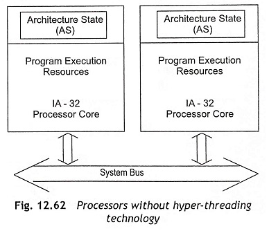
Figure 12.62 shows a system in which there are two physical processors without hyper-threading technology. On the other hand, Fig. 12.63 shows a two-processor system where each unit is capable of hyper-threading technology. Therefore, the system in Fig. 12.63 can be implemented as 4 CPU systems. This scheme has the same performance gains but the cost increase is only 5% due to about 5% die-area size increase.
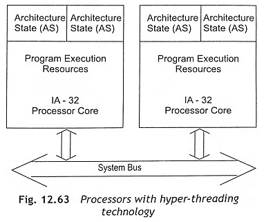
Architecture State (AS) Hyper-threading technology was introduced on the Intel Pentium 4 Xeon TM processor. In this processor, there are two logical processors in a single physical processor. Each logical processor has a complete set of the architecture state.
The architecture state has the following registers:
- Registers including the general-purpose registers
- Control register
- Advanced Programmable Interrupt Controller (APIC) registers
- Machine state registers
Since two architecture states are present in a single physical processor, the processor acts as two processors with respect to software perspective. There are three types of resources in hyper-threading technology such as replicated resources, shared resources, and shared/replicated resources,
Replicated Resources Each processor has general-purpose registers, control registers, flags, time stamp counters, and APIC registers. The content of these registers are used as replicated resources.
Shared Resources Memory and range registers can be independently read/write. Therefore, memory, range registers and data buses are used as shared resources.
Shared/Replicated Resources The caches and queues in the hyper-threading pipeline can he shared or not shared according to the situation.
Logical processors share resources on the physical processor, such as caches, execution units, branch predictors, control logic, and data buses. Each logical processor has its own advanced programmable interrupt controller. Usually, interrupts are sent to a specific logical processor for proper handling.
In most of the applications, multiple numbers of processes or threads may be executed in parallel. This kind of parallel execution is called thread-level parallelism, and these give better performance in online applications such as the server system and Internet applications.
When the current executing process is completed in time-sliced multi-threading, its context will be saved into the memory. Whenever the process starts execution again, the context of the process is again restored to exactly the same state. Therefore, this process consists of the following operations:
- Save the context of the currently executing process after the time slice is over.
- Flush the CPU of the same process.
- Load the context of the new next process, known as context switch.
When the process consists of m number of threads, the total time for context switching will be m times that of a single thread context-switching time. Hence, context switching requires a number of CPU cycles. If multiple numbers of threads are present, system performance will be improved. But a large number of threads consume more time in context switching.
To improve the system performances, the following methods are used:
- Reduce the number of context switches.
- Provide more CPU execution time to each process.
- Execute more than one process at the same time by increasing the number Of CPUs.
- In multiple number of processor systems, the scheduler can schedule two processes to two different CPUs for execution simultaneously. Hence, the process will not be waiting for a long duration to get executed.
In hyper-threading, the concept of simultaneous multi-threading is used. Hence, there is an improvement in the Intel micro-architecture. With increasing the cost of less than 5% in the die area, the system performance is increased by about 25 per cent.
The major advantage of this Architecture of Pentium 4 Processor is appropriate resource sharing of each shared resource. The most commonly used sharing strategies are partitioned resources, threshold sharing, and full sharing. Usually, the sharing strategy is selected based on the traffic pattern, size of the resource, potential deadlock probabilities and other considerations.
To share the resources, there should be one copy of the architecture state for each logical processor, and the logical processors must share a single set of physical resources. Consequently, the operating systems and user programs can schedule processes or threads to logical processors as these processors behave as conventional physical processors in a multi-processor system. According to micro-architecture perspective, instructions from logical processors will carry on execution simultaneously after sharing resources.
Streaming SIMD Extension (SSE), Extension 2 (SSE2) and Extension 3 (SSE3) Instructions
When the MMX instructions are extended incorporating floating-point instructions, the extended instructions are called Streaming SIMD Extensions (SSE) instructions. Initially, SSE instructions are used in Pentium III and then the SSE instruction set has further been enhanced in Pentium 4. The features of SSE instructions are given below:
Streaming SIMD Extensions (SSE) instruction
- SSE instructions are SIMD instructions for single-precision floating-point numbers.
- SSE instructions can be operate on four 32-bit floating points in parallel.
- A set of eight new SIMD floating-point registers are specifically defined for SSE. The SSE registers are named XMM0 through XMM7.
- Each register for SSE is 128 bits long allowing 4 x 32 bit numbers to be handled in parallel.
- As different registers have been allocated, it is possible to execute both fixed-point and floating-point operations simultaneously.
- The SSE instructions can execute non-SIMD floating-point and SIMD floating-point instructions concurrently.
- The SSE instructions can operate on packed data or on scalar data and increase the speed of manipulation of 128-bit SIMD integer operations.
- The SSE instructions can be grouped as data-transfer instructions, data-type conversion instructions, arithmetic, logic and comparison group of instructions, jump or branch group of instruction, data management and ordering instructions, shuffle instructions, cache-ability instructions and state-management instructions.
Streaming SIMD Extension 2 (SSE2) Instructions In Pentium 4, the pipeline depth is increased significantly, and execution rate for all instructions are improved. About 144 new instructions are added with SSE instructions set which allow up to 4 Internet/multimedia based operations in the Pentium 4 processor and these will be executed simultaneously. These new instructions and the other improvements are called Streaming SIMD Extension 2 (SSE2) instructions. The SSE2 instructions support new data types, namely, double-precision floating points. The Intel NetBurst micro-architecture has extended the SIMD capabilities after adding SSE 2.
Streaming SIMD Extension 3 (SSE3) Instructions The Streaming SIMD Extensions 3 (SSE3) instructions have been introduced in the next-generation Pentium 4 processor. This version was developed by Intel in 2004, when the latest version of Pentium 4, the Prescot was released. Actually, the SSE 2 instruction set was extended to SSE3 after adding 13 additional SIMD instructions over SSE2. The SSE3 instructions are used for the following operations:
- Complex arithmetic operations
- Floating-point-to-integer conversion
- Video encoding
- Thread synchronization
- SIMD floating-point operations using array-of-structures format