Pentium Bus Interfacing:
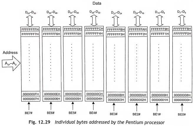
Pentium Bus Interfacing – The Pentium processor has a 64-bit data bus which increases data transfer rates over previous generation processors, and the processor bus is used for connection to a fast L2-cache. The Pentium processor is able to address bytes, word’s and double words as processor instruction set supports bytes, words and double-word type data. This processor uses the byte enable signals, BE7#-BE0#. Each Pentium Bus Interfacing cycle uses address lines A31-A3 to access up to 8 bytes at a time. The byte enable signals BE7#-BE0# is able to address individual bytes as shown in Fig. 12.29.
The Pentium performs the memory accesses as a cache line fills or write-backs. The Pentium processor requires single transfer cycles to I/O device addresses and noncacheable memory areas. Usually, the I/O device address space is 32 bytes wide as I/O device accesses do not work through the D-cache. The I/O subsystem generates A2-A0 signals from BE7#-BE0# for I/O devices which requires address bits A2-A0.
Single Transfer Cycles
In a single transfer read or write cycle, 8 bits, 16 bits, 32 bits or 64 bits of data are transferred to or from the Pentium processor. When the Pentium processor holds CACHE# line at logic level high, it indicates that no line fill operation will be performed. Figure 12.30 shows the single transfer cycle of Pentium processor.
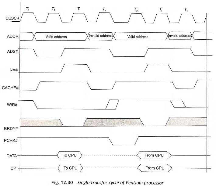
It is clear from Fig. 12.30 that a no-wait single cycle transfer takes at least two CLK cycles. The Pentium processor starts a bus cycle by asserting the Address Status Signal (ADS#) during the first clock pulse (T1) as depicted in Fig. 12.30. The Address Status (ADS#) output signal determines a valid bus cycle and address will be available on the cycle definition pins and the address bus. If the CACHE# output signal is high, the Pentium Bus Interfacing cycle will be a single transfer cycle.
During the second clock pulse of the bus cycle, BRDY# is returned by the external system for a zero wait state transfer. The BRDY# signal is used to detect that the external system has valid data on the data pins due to a read operation, or the external system has received valid data due to a write operation. Actually, the Pentium processor samples the BRDY# input during second clock pulse and subsequent clock pulses of a bus cycle.
The timing diagram of the parity check (PCHK#) output signal and the data parity input are shown in Fig. 12.30. The Pentium processor drives the Data Parity (DP) and returns to the Pentium processor in the same clock as the data. After two clock pulses from BRDY# are returned for reads with the results of the parity, the PCHK# becomes low.
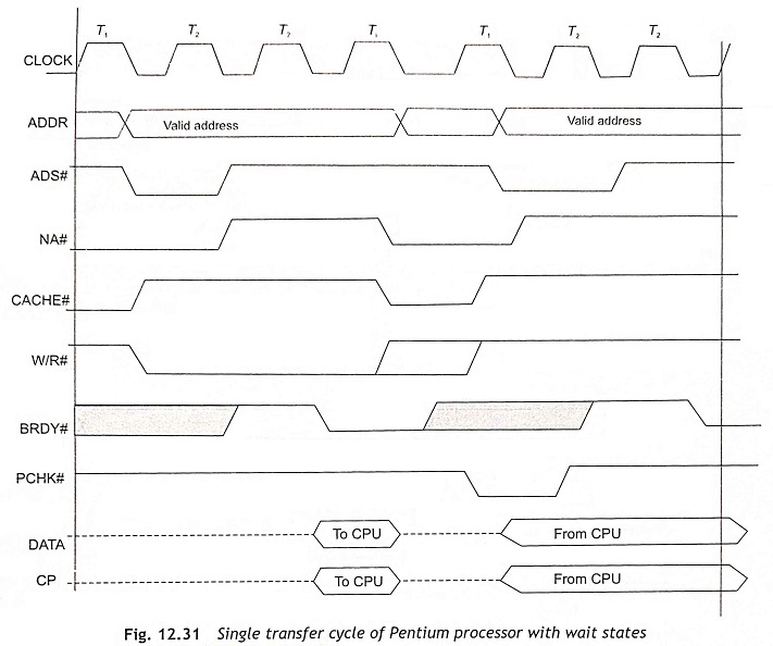
When the Pentium processor is not ready to drive or receive data, wait states must be added to the bus cycle and the BRDY# will not be returned to the processor at the end of the second clock. Figure 12.31 shows a Pentium Bus Interfacing cycles with one and two wait states. At the end of the second clock pulse, BRDY# must be driven inactive. Any number of wait states can be added to Pentium processor bus cycles when BRDY# signal is inactive.
Burst Cycles
If there is a requirement to transfer more than a single data using cacheable and write-back bus cycles. the Pentium processors generally use the burst data transfer technique. During the burst transfers, a new data item can be sampled or driven by the Pentium processor in consecutive clock pulses. The 64-bit data bus of Pentium processors represents 8 bytes. Therefore, a burst is able to transfer 32 bytes within four cycles. The data are contiguous and must be aligned to 32-byte boundaries, equivalent to an internal Pentium processor cache line. Figure 12.32 shows the burst cycle of a Pentium processor.
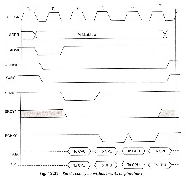
In the burst read cycle, the CACHE# signal becomes low to indicate the memory subsystem that Pentium processor wants to transfer the address into the cache. When the KEN# signal is returned by the memory subsystem as an active low then the Pentium processor extends the single transfer to a cache line fill to store a complete block of data in the on-chip cache.
The burst cycle is also limited to a 32-byte boundary. Therefore, when the first address of data has been sent out, the other three addresses of the next three data are already fixed. This means that the subsystem can independently calculate the other three burst addresses without decoding any other bus addresses from the Pentium processor. Hence, the speed of data transfer will be increased considerably. During the burst cycle, the Pentium processor sends the address ADDR and BEX# signal in the first clock cycle and these signals are not changed after the first clock pulse.
The first address which is sent out by the processor will not inevitably lie on a 32-byte boundary, but can be anywhere in the memory. In the first transfer of the data, the KEN# signal identifies that a burst transfer is going to happen. During the burst transfer stage, the first 8 bytes have already moved out. As a result, the next three cycles should come in a fixed sequence. Actually, the sequence is optimized for the 2-way interleaving of DRAM memory and then the subsystem sends data in a defined order without changing addresses of the processor.
The fastest burst cycle possible needs two clock pulses for the first data item to be returned and all succeeding data items will be returned on each clock pulse. Figure 12.32 shows a burst read cycle without wait or pipelining. When BRDY# is high at the right time, wait states may be inserted into each part of the data transfer.
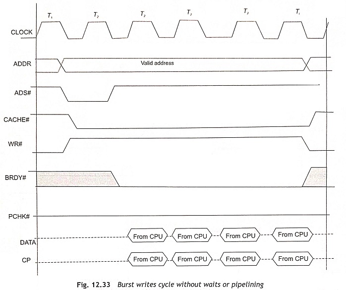
Burst write cycles are always write-backs of modified lines in the data cache. The burst writes always follow the sequence 00H —› 08H —› 10H —› 18H. A burst write is depicted in Fig. 12.33. If there are no wait states, the Pentium processor is able to transfer four bytes in five clocks, called a 2-1-1-1 burst as shown in Fig. 12.33. When a wait state is added in each cycle of data transfer, the burst writes will be known as a 3-2-2-2 burst.
Pentium Address Pipelining
In the Pentium processors, address pipelining can be used to further increase data throughput. For this function, the Pentium uses the NA# signal. Then the first cycle in a bus cycle can be reduced to one clock pulse. The NA# input is used to indicate the Pentium processor that it can drive another cycle before the current one is completed.
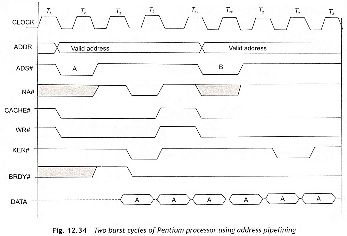
When the memory subsystem has already decoded an address, it is ready to take the next cache-line fill address for decoding if the memory subsystem asserts the NA# signals to the Pentium processor. Then the Pentium processor sends the next address and the subsystem starts the decoding operation of the new address although the third data transfer is still going on. Hence two burst cycles can be done as depicted in Fig. 12.34.
Special Cycles
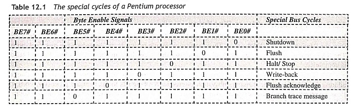
The Pentium processors use control signals to indicate that a special cycle is in progress. The system control signals are D/C#=0, M/IO#=0 and W/R#=1. Usually, the identity of the special cycle is sent out on the byte enable signals BE7#-BE0#. Table 12.1 shows the special cycles of a Pentium processor. When the BRDY# is active low, the external system must take care of special cycles such as Shutdown, Halt/Stop, Flush, Flush Acknowledge, Write-back and Branch Trace Message. INVD and WBINVD instructions are used for flush bus cycle, the WBINVD instruction is applied for write-back bus cycle and FLUSH# must be active low for flush acknowledge bus cycle.
Inquiry Cycles
Generally, multiprocessor-based systems use inquiry or snooping cycles to realize the MESI (Modified, Exclusive, Shared, Invalid) protocol. The external unit can be used to check whether data at a specified address is available in the on-chip cache of the Pentium processor. The external unit can invalidate the stored data and it can also invalidate the whole corresponding cache line.
Usually, any inquire cycle is performed by asserting a HOLD to force the Pentium processor to float its address bus, waiting two clocks, and then driving the inquire address and INV and asserting EADS#. Inquire cycles can be executed if the Pentium processor is forced off the bus due to HLDA or BOFF# signal. Forcefully, the entire cache line is affected by an inquire cycle; address lines A31-A5 will be driven with the valid inquire address. The INV pin must be driven along with the inquire address to indicate whether the line is invalidated or marked as shared. If INV is 1 (high), the line is invalidated. When INV is 0 (low), the line is marked as shared during an inquire hit operation.
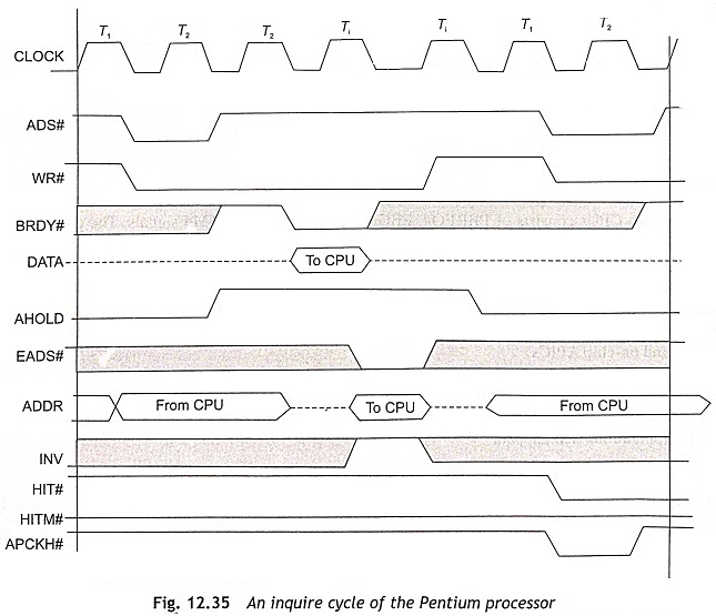
When the Pentium processor finds out that the inquire cycle hits a line either in internal code or data cache, it drives the HIT# pin. Two clocks after EADS# is asserted, HIT# is asserted (0 or low) if the inquire cycle hit a line in the code or data cache as shown in Fig. 12.35. HIT# is de-asserted or high, two clocks after EADS# is asserted if the inquire cycle missed in internal code and data caches. Due to an inquire cycle, the HIT# output changes its value. But HIT# retains its value between inquire cycles. Usually, the HITM# pin is asserted just two clocks after EADS# when the inquire cycle hits a modified line in the data cache. HITM# is low to indicate to the external system that the Pentium processor holds the most recent copy of the data and any device wants to read that data.