Cache Memory in Pentium Processor:
Cache Memory in Pentium Processor – Pentium processors operate at very high clock speeds to provide very good performance. But reading and writing memory off-chip is much slower than accessing CPU registers on-chip. Therefore, the access time of the memory in a system has a critical effect on the system’s performance. Presently, two types of read and write memories, such as dynamic RAMs (DRAMs) and static RAMs (SRAMs), are commonly used in computer systems. DRAMs are very large in size and are relatively cheap. DRAMs are slower as compared to the clock frequency of Pentium processors and it is very difficult to make DRAMs faster. SRAMs are much faster, but they are small in size and more expensive per byte than DRAMs. SRAMs have less access time as compared to the bus speed of the processor. To achieve the benefit of fast access times and also large memory capability in a system, a combination of SRAMs and DRAMs are used. Consequently, the system designer designs a memory system using a compromise combination of SRAMs and DRAMs. The SRAMs within the larger memory system of any computer system is known as the cache memory.
The SRAM is used as Cache Memory in Pentium Processor in the system and DRAM is used within the large memory system. A cache memory is small in size and very easily accessible. Usually, SRAMs are used to hold copies of recently executed instructions and data. The SRAM always operates transparently to the programmer. The cache may be on-chip or off-chip. The on-chip caches are too much faster as the signal delay is much shorter. Therefore, Cache Memory in Pentium Processor works as most successive memory accesses affect only a very small address area. This is called locality. Consequently, at any time the program can be executing the same instructions over and over in a loop or accessing the same areas of data. In this way, the reduced access time over many cycles improves system performance significantly.
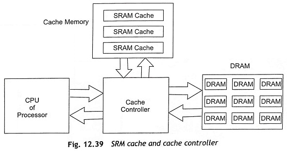
Therefore, code and data should not be placed in the slower main memory. Figure 12.39 shows the block diagram of SRAM cache interfacing with the CPU and cache controller. It is clear from Fig. 12.39 that the fast SRAM cache is placed between the CPU and the slower DRAM through a cache controller. The SRAM cache is used to hold the most frequently accessed instructions as well as data and make it available very quickly. The cache controller controls the complete process. The cache controller uses different strategies such as write-through, write buffering, or modified write-through, and write back to maintain the data in the cache and the main memory.
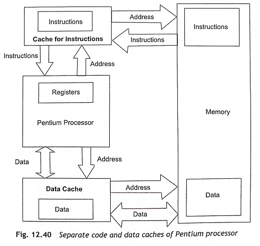
There are two types of cache organization at the highest levels of memory organization. The first is unified cache and other is separate instruction and data caches. The unified cache is commonly used for instructions and data in the 80486. The unified cache is very efficient in terms of the use of the available cache, but it is slower. Pentium and later IA-32 processors use separate instructions and data caches called a Harvard cache. Figure 12.40 shows the separate code and data caches (Harvard cache).
When the Pentium processor wants to read data, it sends out the memory address of desired data. Then cache controller decides whether the address of data is in the SRAM cache or in the main memory. When the data is in the cache, it is called a cache hit and the address is passed to cache memory without delay. The effectiveness of a Cache Memory in Pentium Processor is measured in terms of % cache hits measured against total memory accesses. In case of tightly written code, the cache hit rate can be about 90%. When the processor sends out an address of data which does not exist in the cache memory, it is called a cache miss. Subsequently, the cache controller must go out to the main memory. The proportion of memory accesses which are satisfied by the cache is know as the cache hit rate, and the proportion of memory accesses which are not satisfied by the cache is called the cache miss rate. Usually, the miss rate of a Pentium processor will be a few per cent to remove the memory bottleneck.
When there is a hit, the cache controller reads data from the fast SRAM cache and sends the data to the CPU without any wait states. If there is a cache miss, the cache controller first reads the main memory, so that the read is switched to the main memory. This operation requires wait states so that the cache controller must de-assert the RDY# signal. Subsequently, the processor will insert wait states until the data is available. The cache controller simultaneously controls the cache and main memory. When a cache miss occurs, not only the requested data bytes but also a small block of data, called the cache line, will be read from the main memory into the Cache Memory in Pentium Processor. This process is known as cache line fill. To get best performance, the data bytes which are requested by the CPU for read, must be passed on before the cache line fill is completed.
Generally, cache lines are 32 bytes in size, as data and code exist in blocks within memory. The cache controllers use a burst mode to read cache lines and multiple bus cycles are used to read a large number of bytes. Actually, burst mode almost doubles the bus transfer rate. As a result, a cache line can be read quicker than single values. In this way, cache lines improve the system performance.
When the Pentium processor does a write operation, the cache controller always checks if the data is available in the cache. If so, the data is written to the cache. It is also required to write data in the main memory. For the case of a cache hit, two different strategies such as write-through and write-back are used for this purpose.
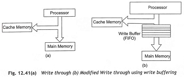
Write through Strategy In a write-through strategy, the CPU always stores data to the main memory for any write operation even though there is a cache hit. All writes are switched through to the main memory as depicted in Fig. 12.41(a). When there is a cache hit, the cache memory will be updated with the new data. The disadvantage of a write-through strategy is that all writes go to the main memory and wait states are inevitable. Therefore, the writing speed becomes slower. By using write buffers (FIFO), the writing speed can be increased up to a certain extent as shown in Fig. 12.41(b). But this process works until the buffers fill up. After filling the FIFO buffer, multiple write operations enter wait states.
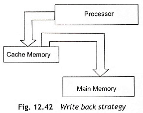
Write-Back Strategy Figure 12.42 shows the write-back strategy. In a write-back strategy, the Cache Memory in Pentium Processor receives all the write operations and updates the cache entry only. The cache lines always remember that they have been modified using a dirty bit on each line. The cache line which has been already changed is only written to the main memory after some specific events. Hence, Pentium processor updates the main memory by the following ways:
- When WBINVD (write-back and invalidate data cache) instruction is executed
- Though hardware signal FLUSH#
- When there is a cache miss, a new cache line is replaced by an old one
- Whenever an internal or external inquiry cycle is executed
The disadvantage of a write-back strategy is that exchanging cache lines takes longer time during exchanging data, as data will be written to the main memory before the new memory is loaded into the cache memory.
Write-allocate In the write-allocate approach, if data is being, written out to main memory, the cache controller should try to cache it even in the case of a cache miss. Consequently, the latest data will be waiting in the cache the next time it is required. Therefore, the cache controller allocates a new cache entry for the write cycle. After that, if the cache is fully used, the new allocation may displace a more useful old cache entry. The main application of the write-allocate strategy is for bus snooping. But the fact is that if there are some cache misses, most caches simply switch through to main memory and just ignore the cache.
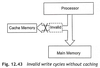
When the processors or DMA controllers can access the main memory, the cache controller must allow the cache that its data become invalid, when the other devices want to write to the main memory. This process is known as cache invalidation. Figure 12.43 shows the invalid write cycles without caching. While the cache controller uses a write-back strategy, there are certain times when the contents of the Cache Memory in Pentium Processor have to be transferred to main memory. For example, a DMA controller wants to write data from the main memory out to a peripheral, but the latest data is only in the cache. This case is called a cache flush.
Cache Organization
A Cache Memory in Pentium Processor is used to store both the data and the address where the data is stored in the main memory. There are methods of cache organization such as direct mapped cache and two-way set-associative cache. In this section, both direct mapped cache and two-way set-associative cache are discussed elaborately.
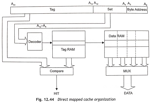
Direct Mapped Cache The simplest cache organization is the direct mapped cache as shown in Fig. 12.44. There features of a direct-mapped cache are given below:
- A specified data or a memory item is stored in a unique location in the cache memory and two items with the same cache address will compete for use of that location. For example, when a cache line is already placed at an address in the Cache Memory in Pentium Processor, we also want to put another cache line at another address in the cache memory. These two addresses should have the same A12-A4 address bits all the time. Therefore, these addresses cannot both be placed in the cache at the same time. This is known as contention.
- Those bits are not used to select within the line or to address the cache RAM, these bits will be stored in the tag field.
- The tag and data access can be performed simultaneously and also provide the fastest cache access time of any organization.
- The tag RAM is always smaller than the data RAM. Hence, the access time of the tag RAM is shorter than data RAM and the tag comparison can be completed within the data access time.
- The direct mapped cache organization can store 8 Kbytes in 16-byte cache lines. The direct mapped cache has 9 address bits A12-A4 or 512 lines. The first 4bits (A3-A0) of the 32-bit address bus A31-A0 are used to address the bytes within the line and there are 19 tag bits (A31-A13). Therefore, 512 x 19 (9728) bits are required for storing the tag.
- While data is loaded into the Cache Memory in Pentium Processor, a block of data will be fetched from memory using burst cycles. Normally, line size is not smaller than the block size. When the block size is smaller than the line size, a valid bit will be used to indicate each block within the line. To get the simplest cache organization, the line will be equal to block size.
Two-Way Set-Associative Cache To reduce the problems due to contention, the set-associative cache is used by allowing a particular memory item to store in more than one cache location. Figure 12.45 shows the 2-way set-associative cache organization. In this cache organization, two direct-mapped caches work in parallel. The address applied to the cache may find its data and each memory address can be stored in one of the two places. Each of the two items, which were in contention for a single location in the direct-mapped cache organization, may be stored at one of the two places after allowing the cache to hit on both.
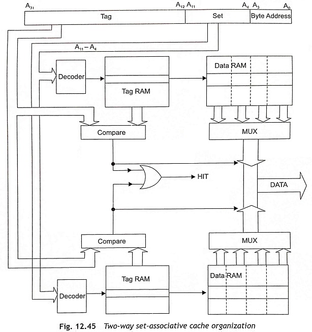
The two-way set-associative caches have 8 Kbyte caches with 16-byte cache lines and eight address bits A11-A4 and 256 lines in either half of the cache. Therefore, four bits of the 32-bit address, A3-A0, are used to select a byte from the cache line and eight bits A11-A4 are used to select one line from each half of the cache. Consequently, there are 20 address bits A31-A12 for the address tag. The access time of a two-way set-associative cache is slightly larger than the direct-mapped cache as the extra time is required to perform the multiplexing operation.
Cache Consistency
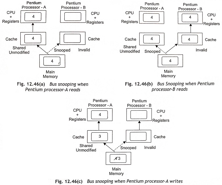
The cache consistency problem occurs when data can be modified by more than one source. When a copy of data is held in both main memory and a cache memory, one copy is changed and the other copy is stale and the system consistency will be lost. If there are two caches in the system, the problem becomes very complicated. Assume a multiprocessor system consists of two processors, namely, Pentium-A and Pentium-B. If the secondary Pentium processor (Pentium-B) overwrites a common memory location, the other processor (Pentium-A) should know that this has occurred. Usually, the MESI protocol for cache lines is used in Pentium and advanced processors to ensure cache consistency. Figure 12.46 shows the bus snooping when two processors each with a local cache have access to a common main memory.
MESI (Modified, Exclusive, Shared, Invalid) Protocol
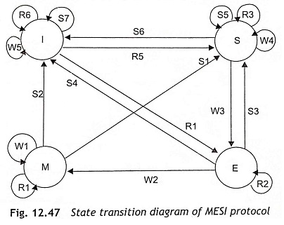
The abbreviation of MESI is Modified, Exclusive, Shared, and Invalid, which are the four possible states of a cache line. The MESI protocol is a general mechanism to control cache consistency, using snooping techniques. The Pentium processors can change the state of a cache line through read or write cycles or internal snooping and other devices such as L2-cache controller can change the state through external snooping. The MESI protocol provides each cache line that can be one of the four states, and the MESI protocol is managed by the two MESI bits. Figure 12.47 shows the state transition diagram of MESI protocol. The modified, exclusive, shared, and invalid stages of the protocol are explained in this section.
Modified (M) When the data of a cache line is marked as modified (M), it is available in a single cache of the complete system only. This cache line can be read or written to without an external cycle.
Exclusive (E) The exclusive (E) cache line is always stored in only one of the caches in a computer system, though it has not been modified. Hence its values are the same as in the rest of the system. The cache line can be read or written to without an external cycle. Once it is written, to the cache line should be set to modify.
Shared (S) The shared (S) line can be stored in other caches of the system. The shared line always has the current value so that read accesses can be obtained from the cache. Write accesses to a shared cache line are switched through the external data bus, whenever any cache write strategy is used. Therefore, the shared cache lines in the other caches are invalidated.
Invalid (I) The cache line which is marked as invalid is not available in the cache. The catch lines marked as invalid (I) lines might be empty or could have invalid data in the cache. Each access to an invalid cache line generates a cache miss. During read access, the cache controller starts a catch line fill and the cache controller switches the write through to the external bus, rather than a write-allocate.
It is clear from the state transition diagram of MESI protocol that there are six read access states, R1 to R6; five write access states, W1 to W5, and seven inquiry or snooping states S1 to S7. The function of each state is given below:
Six Read Access States R1 to R6
- R1 Read access leads to a hit. Data is available in the cache and it is transferred to the CPU of Pentium processor (M←M).
- R2 Read access leads to a hit. Data is available in the cache and it is transferred to the CPU of Pentium processor (E←E).
- R3 Read access leads to a hit. Data is available in the cache and it is transferred to the CPU of Pentium processor (S←S).
- R4 Read access leads to a miss. Data is not available in the cache. The cache controller performs an external read and a line fill (E←I).
- R5 Read access leads to a miss. Data is not available in the cache. The cache controller performs an external read and a line fill (S←I).
- R6 Read access leads to a miss. Data is not available in the cache. The cache controller is not able to perform a line fill and the cache line remains invalid (I←I).
Five Write Access States, W1 to W5
- W1 Write access leads to a hit. Data is available in the cache. As MESI protocol operates with write-back cache strategy, no write cycle is sent to the external bus (M←M).
- W2 Write access leads to a hit. Data is available in the cache and it was not previously overwritten. As MESI protocol operates with write-back cache strategy, no write cycle is sent to the external bus (M←E).
- W3 Write access leads to a hit. Data is available in the cache but it was shared. The cache controller sends a write cycle to the external bus. Then cache line is used in one cache. The main memory is updated, and the cache becomes exclusive (E←S).
- W4 Write access leads to a hit. This state will operate for a write-through cache. At this time, all writes switched to external bus and the cache line stay as shared (S←S).
- W5 Write access leads to a miss. Data will be written to the main memory, but not in the cache. The cache line remains invalid (I←I).
Seven Inquiry or Snooping States, S1 to S7
- S1 The snooping (inquiry) cycle hits a modified cache line. The reference cache line will be written back to main memory (S←M).
- S2 The snooping (inquiry) cycle hits a modified cache line and this state becomes invalidated. The reference cache line is written back to main memory anyway (I←M).
- S3 The snooping (inquiry) cycle hits an exclusive cache line. This state has not been modified and it does not require writing back to main memory. The content of main memory is written to another cache line and the previously exclusive line is now shared (S←E).
- S4 This snooping (inquiry) cycle hits an exclusive cache line. This state has not been modified and does not need to write back to main memory. The content of the main memory is written to another cache line. Due to some reason, this line becomes invalidated (I←E).
- S5 The snooping (inquiry) cycle hits a shared cache line. This snooping cycle informs the system that this cache line is available in the cache (S←S).
- S6 The snooping (inquiry) cycle hits a shared cache line. For some reason, this line will be invalidated (I←S).
- S7 The snooping (inquiry) cycle hit an invalid cache line (I←S).
L2 Caches and MESI Protocol
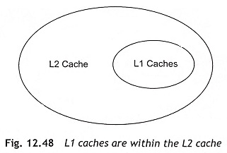
Generally, L1 caches are small in size and available as local. L2 caches are larger in size but a little bit slower. Presently, L2 caches are available on-chip Pentium processors. For example, L1 cache of Pentium-II processor can provide data in one cycle, but L2 cache takes two cycles to supply data. The Modified, Exclusive, Shared, and Invalid (MESI) protocols can be applied to the multicache system. The cache consistency can be achieved when all the addresses in the L1 cache are available in the L2 cache as depicted in Fig. 12.48. The data in the two caches may not be the same as the L1 cache may be a write-back cache.
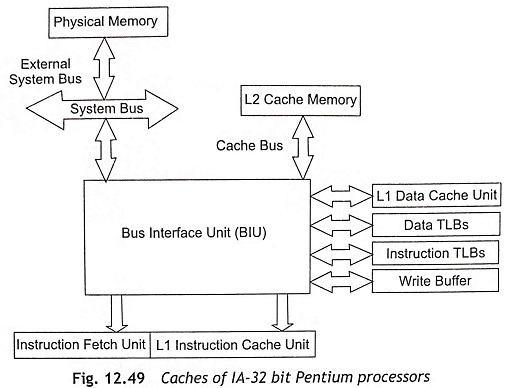
The data transfer between the CPU and main memory takes place over the L2 cache. The MESI protocol can be performed over the three stages such as (i) L1 cache, (ii) L2 cache, and (iii) main memory. The MESI state of an L2 cache line always operates one step ahead of the MESI state of the related L1 cache line. An inquiry or snooping cycle is used by the L2 cache to decide whether a certain cache line is available in the L1 cache and it has been changed. If there is an inquiry cycle in a modified line, the L2 cache will be updated by a write-back cycle to the L2 cache. After that, the L2 cache can also ask for a back-invalidation cycle and this can indicate to the hit line being made invalid. Figure 12.49 shows the caches of IA-32 bit Pentium processors.
Pentium On-Chip Caches
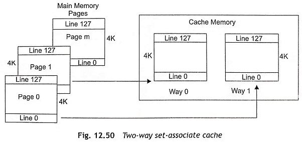
The Pentium processor supports an 8 Kbyte data cache and an 8 Kbyte code cache. The data cache (D-cache) is used to store data and the instructions are stored in code cache (I-cache). The code and data caches are two-way set-associative. Both D and I caches can be accessed simultaneously. The code cache provides up to 32 bytes of opcodes, but the data cache provides data for two data references in the same clock pulse. Both caches are parity protected. The cache page size is 4K or 128 lines and the cache line size is 32 bytes. Each cache line is filled by a burst of four read cycles though the processor’s 64-bit data bus. The two-way set-associate scheme consists of two different ways such as Way 0 and Way 1 as shown in Fig 12.50. Each cache way contains 128 cache lines.
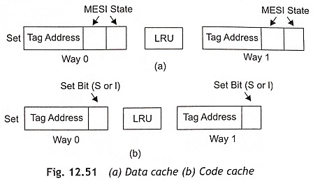
The code cache is write-protected to prevent code corruption. The code cache can support the two states of the MESI protocol, namely, the S and I states. The data cache fully supports the MESI protocol. The data cache is configurable as write-back or write-through strategy. Memory areas can be defined as noncacheable by external hardware or software. Cache line consistency as well as replacement can be done using hardware. Usually, the LRU method is used for cache line replacement in both the data-cache and code-cache. This LRU method requires one bit per set in each of the caches. Figure 12.51(a) shows the data cache and the code cache is depicted in Fig. 12.51(b).
Physical Addresses Data cache and code cache can be accessed by a physical address. Therefore, each cache has its own TLB to translate linear addresses to physical addresses. For example, the data cache has separate TLBs for 4 Kbyte and 4 Mbyte pages, but the code cache has only one TLB for both 4 Kbyte and 4 Mbyte pages. Actually, the TLBs are 4-way set associative caches.
Cache Operating Modes The cache operating modes are controlled by the CD and NW bits of CR0 register. For normal operation and best performance, CD = 0 and NW = 0. When both CD and NW bits are set to 1 after reset. When both CD and NW are 0, the cache performs the following operation:
- Read hits access the cache.
- Read misses cause line fills.
- Enter the Exclusive (E) or Shared (5) state under the control of the WB/WT# signal.
- Write hits update the cache.
- Write to shared lines and write misses will appear externally.
- Write to shared lines will be changed to the Exclusive (E) state under the control of WB/WT# signal.
- Inquire or snooping cycles are performed.
To disable the cache, the following operations are required:
- Set the CD and NW bits. Therefore CD = 1 and NW = 1.
- Flush the caches.
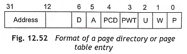
Page Cache-ability Figure 12.52 shows the format of a page directory or page-table entry. To control page-cache ability, page directory and page table entries have two bits, namely, PWT (Page Write Through) and PCD (Page Cache Disable). The states of these bits are placed on the PWT and PCD pins during memory access cycles. The PWT bit controls write strategy for the external L2 caches. When PWT = 1, a write through strategy for the current page is used. If PWT = 0, a write-back strategy is used for the current page. The PCD bit controls cache ability on a page-by-page basis. The PCD bit is logically ANDed with the KEN# signal to control cache-ability on a cycle-by-cycle basis. When PCD = 0, this bit enables page caching operation. If PCD = 1, it disables page caching operation. The Cache line fills are enabled if PCD = 0 and KEN# = 0.
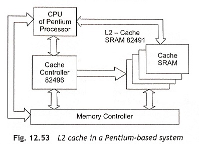
Pentium L2 Cache Intel has developed a 82496 cache controller for the Pentium processors to operate with the cache SRAM modules (82491) which work as an L2cache in the system. The 82496 cache controller is used to implement the MESI Protocol for the L2 caches. This cache controller may be configured as an L2 cache with 256 Kbyte or 512 Kbyte size. The 82496 cache controller implements a two-way set-associative cache organization which can support cache line sizes of 32, 64 and 128 bytes.