Voltage Multipliers – Voltage Doublers, Triplers and Quadruplers
Voltage multipliers is a modified capacitor filter circuit that delivers a dc voltage twice or more times of the peak value (amplitude) of the input ac voltage. Such power supplies are used for high-voltage and low-current devices such as cathode-ray tubes (the picture tubes in TV receivers, oscilloscopes and computer display). Here we will consider half-wave voltage doubler, full-wave voltage doubler and voltage tripler and quadrupler.
Half-Wave Voltage Doubler:
The circuit of a half-wave voltage doubler is given in Fig. 9.27. During the positive half cycle of the ac input voltage, diode D1 being forward biased conducts (diode D2 does not conduct because it is reverse biased) and charges C1 up to peak value of secondary voltage VS max with the polarity, as marked in Fig. 9.27. During the negative half cycle of the input voltage diode D2 gets forward biased and conducts charging capacitor C2. For the negative half cycle, the lower end of the transformer secondary is positive while upper end is negative. The polarity of C2 has also been marked in the figure. Now starting from the bottom of the transformer secondary and moving clockwise and applying Kirchhoff’s voltage law to the outer loop we have
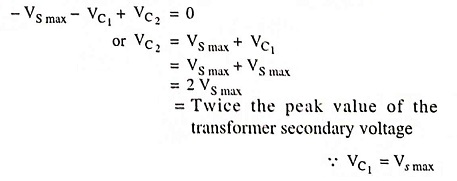
During the next positive hall cycle diode D2 is reverse biased and so acts as an open and capacitor C2 discharges through the load. If there is no load across the capacitor C2 both capacitors stay charged – C1 to VS max and C2 to 2 VS max. If, as expected, there is a load connected to the output terminals of the voltage doubler, the capacitor C2 discharges a little bit and consequently the voltage across capacitor C2 drops slightly. The capacitor C2 gets recharged again to 2Vmax during the negative half cycle. The output waveform across capacitor C2 is that of a half-wave signal filtered by a capacitor filter in the next half cycle. The ripple frequency in this case will be signal frequency (i.e., 50 Hz for supply mains). The peak inverse voltage across each diode is 2 VS max. The half-wave voltage doubler is used to provide a dc output voltage of the order of 3 kV.
Full-Wave Voltage Doubler:
The circuit diagram for a full-wave voltage doubler is given in Fig. 9.28. During the positive cycle of the ac input voltage, diode D1 gets forward biased and so conducts charging the capacitor C1 to a peak voltage VS max with polarity indicated in the figure, while diode D2 is reverse biased and does not conduct. During the negative half cycle, diode D2 being forward biased conducts and charges the capacitor C2 with polarity shown in the figure while diode D1 does not conduct. With no load connected to the output terminals, the output voltage will be equal to sum of voltages across capacitors C1 and C2 i.e.,VC1 + VC2 or (VS max + VS max) or 2 VS max. When the load is connected to the output terminals, the output voltage VL will be somewhat less than 2 VS max. The input voltage and output voltage waveforms are also shown in Fig. 9.28.
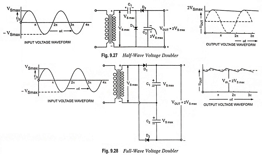
It is seen that half-wave or full-wave voltage doubler circuits provide twice the peak voltage of the transformer secondary while requiring no centre-tapped transformer and only 2 VS max PIV rating for diodes.
The advantage of a full-wave voltage doubler over an half-wave voltage doubler is that the output ripple frequency is twice the supply frequency and it is easier to filter high frequency ripples. The drawback of a full-wave voltage doubler is that common ground between input and output is not available.
Voltage Tripler and Quadrupler:
The half-wave voltage doubler, shown in Fig. 9.27 can be extended to provide any multiple of the peak input voltage (i.e., 3VS max, 4VS max or 5VS max), as illustrated in Fig. 9.29. It is obvious from the pattern of the circuit connections how additional diodes and capacitors are to be connected to provide output voltage, 5, 6, 7 or 8 times the peak input voltage from a supply transformer of rating only VS max, and each diode in the circuit of PIV rating 2 VS max. If load is small and the capacitors have little leakage, extremely high dc voltages can be obtained from such a circuit using many sections to step up the dc voltage.
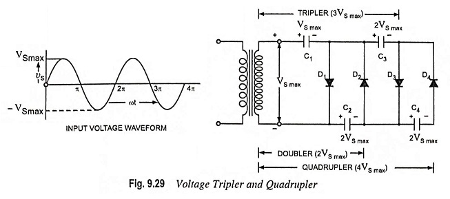
In operation, capacitor C1 is charged through diode D1 to a peak value of transformer secondary voltage, VS max during first positive half cycle, of the ac input voltage. During the negative half cycle capacitor C2 is charged to twice the peak voltage 2 VS max developed by the sum of voltages across capacitor C1 and the transformer secondary. During the second positive half cycle, diode D3 conducts and the voltage across capacitor C2 charges the capacitor C3 to the same 2 VS max peak voltage. During the negative half cycle diodes D2 and D4 conduct allowing capacitor C3 to charge capacitor C4 to peak voltage 2 VS max. From Fig. 9.29 it is obvious that the voltage across capacitor C2 is 2 VS max, across capacitors C1 and C3 it is 3 VS max and across capacitors C2 and C4 it is 4 VS max.
If additional diodes (each diode of PIV rating 2 VS max) and capacitors (each capacitor of voltage rating 2 VS max) are used, each capacitor will be charged to 2 VS max. Measuring from the top of the transformer secondary winding (Fig. 9.29) will give odd multiples of VS max at the output, while measuring from the bottom of transformer secondary winding will give even multiples of the peak voltage, VS max.
Some electronic devices, such as cathode-ray tubes (in picture tubes in TV receivers, oscilloscopes and computer display) needs dc power supply at high voltage with low current. This requirement can be met with either by employing a step-up transformer with a rectifier circuit or by employing voltage multipliers. Since transformers are very bulky and costly, voltage multipliers are preferred. By using voltage multipliers, the voltage level is usually raised well into the hundreds or thousands of volts.
Generally such circuits are employed when both the supply voltage and load are maintained constant.