Internal Architecture of Pentium Processor:
The Pentium is a 32-bit processor, but it has a 32-bit address bus and a 64-bit data bus. This processor’s data bus serves the on-chip caches, but not the 32-bit registers. The internal and external data buses are connected through the caches. Figure 12.1 shows the internal architecture of Pentium processor which consists of 8K byte code cache, 8K byte data cache, Translation Look-aside Buffer (TLB), Branch Trace Buffer (BTB), Integer pipelines U and V, floating-point pipeline, Microcode ROM, and Control Unit (CU).
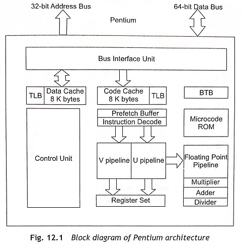
Code and Data Cache There are separate code and data caches, and the cache line size is 32 bits just like the 80486 processor. Each cache is connected with its own Translation Look-aside Buffer (TLB). Therefore, the paging unit of the Memory Management Unit (MMU) can rapidly convert linear code or data addresses into physical addresses. Due to two separate caches, the pre-fetches cannot conflict with data access cycles.
Branch Prediction Branch prediction consists of a Control Unit (CU) and a Branch Trace Buffer (BTB). The function of control unit and Branch trace buffer are as follows:
Branch Trace Buffer (BTB) The BTB is used to store the target address and statistical information about the branch operation. Hence, the branch prediction is able to predict branches and cause the Pentium to use the most likely target address for instruction fetching. Pipeline freeze up caused by pipeline flushes and the subsequent fetching operations are reduced and the program execution is accelerated
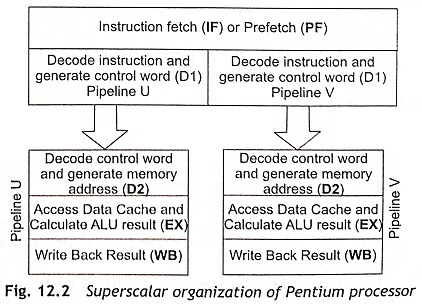
Control Unit (CU) The control unit controls the five-stage integer pipelines U and V, and the eight-stage floating-point In the Architecture of Pentium Processor, the integer pipelines are used for all instructions which are not involved in any floating-point operations. Therefore, the Pentium can transmit two integer instructions in the same clock cycle and performance of the processor is improved. This method is called superscalar architecture, Figure 12.2 shows the superscalar organization of the Pentium processor.
The first four stages of the floating-point pipeline overlap with the U pipeline and the parallel operation of the integer and floating-point pipelines is possible only under some specified conditions. If the operating clock frequency of Pentium is same as 80486, the Pentium floating-point unit is able to execute floating-point instructions 3 to 5 times faster than 80486. This is possible as a hardware multiplier, divider and quicker algorithms are incorporated in the microcode floating-point unit.
The Pentium has a microcode support unit to support complex functions. The support unit controls the pipelines with the microcode. Actually, this unit uses both pipelines together. Therefore, complex microcode instructions run very fast on a Pentium than on a 80486.
Integer Pipelines U and V
The Pentium is a superscalar processor and it has two integer pipelines, called U and V. The process of issuing two instructions in parallel is known as pairing.
The U-pipeline is able to handle the full instruction set of the Pentium but the V-pipeline has limited handling capability. The
V-pipeline is able to handle only simple instructions without any microcode support. The V-pipeline is used to execute ‘simple integer instructions’ such as load/store type instructions and the FPU instruction FXCH, but the U-pipeline executes any legitimate Pentium instructions. Actually, Architecture of Pentium Processor use a set of pairing rules to select a simple instruction which can go through the V pipeline. When instructions are paired, initially the instruction is issued to the U-pipe and then the next sequential instruction is issued to the V-pipe.
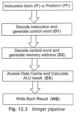
There are two integer pipelines and a floating-point unit in the Architecture of Pentium Processor. Figure 12.3 shows an integer pipeline. Each integer unit has the basic five-stage pipeline as given below:
- Prefetch (PF)
- Decode-1 (D1)
- Decode-2 (D2)
- Execute (E)
- Write Back (WB)
Prefetch (PF) In the prefetch stage of integer pipeline of the Pentium processor, instructions are fetched from the instruction cache as instructions are stored initially in the instruction cache. After fetching, the CPU aligns the codes properly. As the instructions are of variable lengths, the initial opcode bytes of each instruction must be properly aligned. After completion of the prefetch stage, the decode stages D1 and D2 will be executed.
Decode-1 (D1) In the decode-1 (D1) pipeline stage, the CPU decodes the instruction and generates a control word. The D1 pipeline stage has two parallel instruction decoders. These implement the pairing rules. Only a single control word may be sufficient to start execution of the data transfer, arithmetic and logical operations in RISC processor. This processor supports complex CISC instructions with the help of microcoded control sequencing.
Decode-2 (D2) The decode-2(D2) pipeline stage is required whenever the control word from D1 stage is decoded to complete the instruction decoding. In this stage, the CPU generates addresses for data memory.
Execute (E) The execution stage is used for both ALU operations and data cache access. The data cache is used for data operands and ALU performs arithmetic logic computations or floating-point operations. In the execution stage, all U-pipe and V-pipe instructions, except conditional branches, are verified for correct branch prediction. A microcode is designed to use both the U and V pipes. Therefore, microcode instructions are executed faster on the Pentium than on the 80486.
Write Back (WB) The final stage of the five-stage pipeline is Write Back (WB). In the WB stage, the CPU updates the contents of registers and status of the flag register after completion of execution. In this stage, the V-pipeline conditional branch instructions are verified for correct branch prediction.
The Pentium pipeline structure is similar to 80486 pipeline structure. Usually, the 80486 takes two clock cycles to decode instructions, but the Pentium processor takes only one clock cycle as Pentium processor has an additional integrating hardware in each pipeline stages to speed up the process.
Superscalar
The Internal Architecture of Pentium Processor has been designed based on Superscalar. In Superscalar architecture, two instructions are executed in parallel. Figure 12.2 shows the superscalar architecture. Two independent integer pipelines are depicted in Fig. 12.2. In the PF and D1 stages, the microprocessor can fetch, instructions decode instructions and generate control words. In this stage, decoded instructions issue them to two parallel U and V pipelines. For complex instructions, D1 generates microcoded sequences for U and V pipelines. Several techniques are used to resolve the pairing of instructions.
Floating-Point Unit
The 80486DX CPU is the first processor in which the 80387 math co-processor has been incorporated on-chip to reduce the communication overhead. The 80486 CPU contains a floating-point unit, but this floating-point unit is not pipelined. The Architecture of Pentium Processor has been designed for incorporating on the chip numeric data processor.
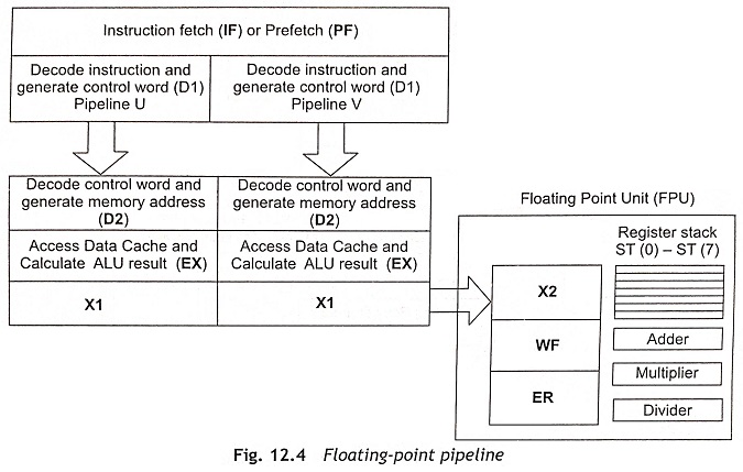
The Floating-Point Unit (FPU) of Pentium has an eight-stage pipeline as shown in Fig. 12.4. The eight pipeline stages are
- Prefetch (PF)
- Decode-1 (D1)
- Decode-2 (D2)
- Execute (dispatch)
- Floating Point Execute-1 (X1)
- Floating Point Execute-2 (X2)
- Write Float (WF)
- Error Reporting (ER)
The first five stages of the pipeline are similar to the U and V integer pipelines. During the operand fetch stage, the FPU fetches the operands either from the floating-point register or from the data cache. The floating-point unit has eight general-purpose floating point registers. There are two execution stages in Pentium such as the first execution stage (X1 stage) and the second execution stage (X2 stage). In the X1 and X2 stages, the floating-point unit reads the data from the data cache and executes the floating-point calculation.
Prefetch (PF) The prefetch stage is same as the integer pipeline of Pentium processor.
Decode-1 (D1) The decode-1 (D1) pipeline stage is also same as the integer pipeline of Pentium processor.
Decode-2 (D2) The decode-2 (D2) pipeline stage is worked as required whenever the control word from D1 stage is decoded to complete the instruction decoding. In this stage, it is the integer pipeline of Pentium processor.
Operand Fetch During the execution stage (E), the floating-point unit accesses the data cache and the floating-point register to fetch operands. Before writing the floating-point data to the data cache, the floating-point unit converts internal data format into appropriate memory representation format.
Floating Point Execute-1 (X1) In the Floating Point Execute-1 (X1) stage, the floating-point unit executes the first steps of the floating-point calculations. While reading the floating-point data from the data cache, the floating-point unit writes the data into the floating-point register.
Floating Point Execute-2 (X2) During the Floating Point Execute-2 (X2) stage, the Floating Point unit execute the remaining steps of the floating-point computations.
Write Float (WF) In the Write Float (WF) stage, the floating-point unit completes the execution of the floating-point calculations and then writes the computed result into the floating-point register file.
Error Reporting (ER) In the error reporting(ER) stage, the floating-point unit generates a report about the internal special situations and updates the floating point status.
The floating-point unit of Pentium consists of a dedicated adder, multiplier and division units. All independent circuits are used to perform addition, multiplication, division and other mathematical operations within very few clock cycles.
The block diagram of the floating-point unit is depicted in Fig. 12.5. There are five segments such as Floating-point Adder Segment (FADD), Floating-point Multiplier Segment (FMUL), Floating-point Divider Segment (FDIV), Floating-point Exponent Segment (FEXP) and Floating-point Rounder Segment (FRD) in the floating-point unit of Pentium processors. These segments are used to perform five different floating-point computations. In this section, the functions of the above segments are discussed.
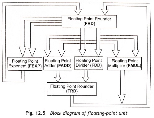
Floating-point Adder Segment (FADD) The floating-point adder segment is used for addition of floating- point numbers and execution of floating-point instructions such as addition, subtraction and comparison. During X1 and X2 stages of the pipeline, the FADD segment is active and executes floating-point instructions based on single-precision, double-precision and extended precision data.
Floating-point Multiplier Segment (FMUL) The floating-point multiplier segment executes floating-point multiplication in single-precision, double-precision and extended precision modes.
Floating-point Divider Segment (FDIV) This segment performs the floating-point division and executes square-root instructions.
Floating-point Exponent Segment (FEXP) The floating-point exponent segment calculates the floating-point exponent. This segment communicates with all other floating-point segments for proper adjustment of mantissa and exponent fields in the final stage of a floating-point computation.
Floating-point Rounder Segment (FRD) After the floating-point addition or division operations, it is required to round off the computed results before write back to the floating-point registers. The floating-point rounder segment is used to perform the round-off operation before write-back stage.
Floating-Point Exceptions
There are six possible floating-point exceptions in Pentium processors during integer arithmetic computations. The six different floating-point exceptions are divide by zero, overflow, underflow, denormal operand and invalid operation. The divide-by-zero exception invalid operation exception and denormal operand exception may be detected before the actual floating-point computation.
The Safe Instruction Recognition (SIR) mechanism is used in a Architecture of Pentium Processor to determine that any floating-point operation can be executed without creating any exception. Whenever an instruction can be executed safely without any exception, the SIR mechanism can he used to allow the instruction for execution. When a floating-point instruction is not safe, the pipeline halts the instruction for three cycles and the exception is generated.
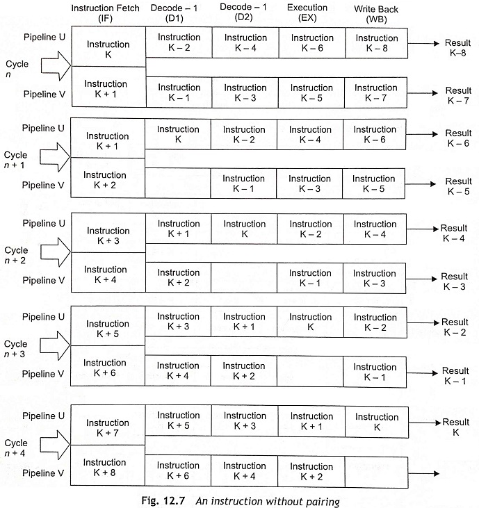
Instruction Pairing
Initially an instruction is loaded into the U pipeline. After that the next instruction will be loaded into V and it must be part of a pair. As per the Pentium processor’s pairing rules, if it is not part of a pair then it cannot be loaded into the V pipeline. Then the instruction has to wait till the next slot is available in the U-pipeline. Usually, the instruction decoding and pairing decisions are done in hardware.
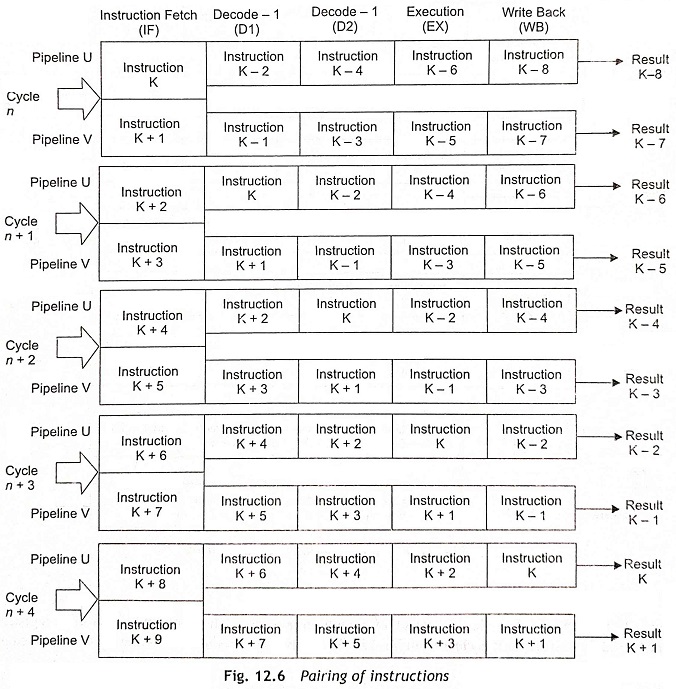
The Pentium pipeline must be transparent to programmers. Whenever the compiler is aware of the Pentium pipeline strategy then instruction throughput can be improved. Figure 12.6 shows the instruction pairing in a Pentium processor. Figure 12.7 shows the example where an instruction cannot be paired.
Pentium Register Set
Figures 12.8(a) and (b) show the register set of a Pentium processor. The Pentium has the same register sets as the 80386 processor, but it is clear from Fig 12.8(b) that two new registers CR4 and TR12 are added in the register set of Pentium processor.
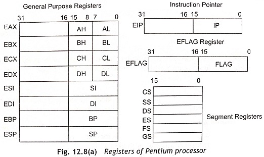
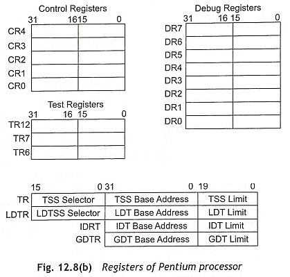
The control register CR4 controls the Pentium processors extensions for virtual-8086 mode operation. The CR4 register is also used for debugger support and it is used to support up to 4 Mbyte pages. The test control register TR12 enables the selective activation of new features of Pentium processors such as branch prediction, and superscalar operation, etc.
Three new flags are also added in the EFLAGS register of Pentium processor. Two flags are used to support virtual 8086 mode operation and the third flag indicates if the processor supports the CPU ID instruction. When the processor can set and clear the ID flag, it can execute the CPUID instruction.