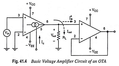
OTA Voltage Amplifier Circuit Diagram:
A basic OTA voltage amplifier circuit diagram is shown in Fig. 41.4.
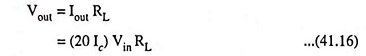
At room temperature (T = 300 K), the output current,
![]()
Now, if the whole output current Iout flows into the RL. This will occur only if [IB+ ≪ Iout], thus
Thus, the RL also contributes to voltage gain. And to have IB+ ≪ Iout, we select an op-amp voltage follower to avoid loading effects.
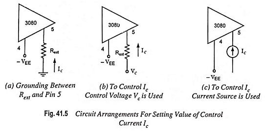
The controlling current Ic also alters the output, so we connect an external resistance Rext (between pair 5 and ground, as shown in Fig. 41.5 (a) so that
![]()
One approach, as shown in Fig. 41.5 (b), to set controlling current lc is using a control voltage Vc, so that
Another approach for setting controlling current Ic is by using a current source, as shown in Fig. 41.5 (c). (One may employ FET, BJT, an op-amp, an lc current chip or another 3080 as current source).