Blocking Oscillator – Definition, Operation and Types:
The output of an active device may be coupled back to the input through a pulse transformer. If the relative windings polarities are properly chosen, the feedback will be regenerative and the circuit can be made to generate a single pulse (monostable operation) or a pulse train (astable operation). A transformer-coupled configuration of considerable importance, known as the blocking oscillator, will be discussed in this section.
Types of Blocking Oscillator:
There are two types, namely
- Monostable Blocking Oscillator
- Astable Blocking Oscillator
Monostable Blocking Oscillator:
The blocking oscillator shown in Fig. 31.52 consists of a transistor with an emitter resistor RE and a 3-winding pulse transformer. One winding is in the collector circuit, the second winding with n times as many turns, is in the base circuit, the third winding, with n1 times as many turns as the collector winding, feeds a resistor RL, which may be the load or may be required for damping. The base and collector turns must be connected for regenerative feedback, but the relative winding polarity of the third leg of the transformer is arbitrary. It may be chosen to provide either a positive or negative output pulse across the load. The emitter resistor RE controls the pulse duration. Since VBB << VCC and does not basically affect the oscillator operation, it may be neglected in discussion.
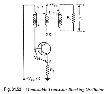
In the quiescent state, the transistor is off. VBB is of the order of a few tenths of a volt. Even though it can be zero, it is chosen as a fraction of volt in order to avoid free running operation at elevated temperatures and to avoid false triggering due to noise spikes. When a triggering signal is momentarily applied at the collector to lower its potential, by transformer action and with the winding polarities as indicated, the base potential rises.
When the base-to-emitter voltage exceeds the cutin voltage, the transistor comes out of cutoff. This makes the collector current to flow, further causing decrease in the collector potential, which in turn causes increase in the base potential. If the loop gain is more than unity, regeneration takes place and the transistor is quickly driven into saturation. During the saturation period, when the collector voltage is constant, the collector current continues to increase at a constant rate due to transformer inductance. The emitter current is virtually constant and is determined by the transformer feedback and the emitter circuit resistor RE. Thus, the base current continues to fall at a constant rate. When the base current is no longer sufficient, the transistor comes out of saturation and regeneration cuts off the transistor. The pulse duration depends upon RE.
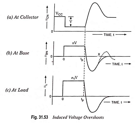
Since the current through the inductor cannot change instantaneously, its current must continue to flow even after the transistor currents have dropped to zero. The path of the magnetizing current is through the capacitance of the transformer (not shown in the figure). Since this capacitance is small, the magnetizing current decays rapidly and thus induce large voltage overshoots at the collector, base and load, as depicted in Figs. 31.53 (a), (b), (c). The load resistance RL assists in damping the overshoots.
Astable Blocking Oscillator:
One form of astable or free running blocking oscillators is obtained by adding R1C1 network in the emitter circuit of a monostable blocking oscillator, as shown in Fig. 31.54. This circuit differs from that of Fig. 31.52 not only in the addition of R1C1 but also in the reversal of the polarity of VBB. Qualitatively the operation of the circuit is as follows.
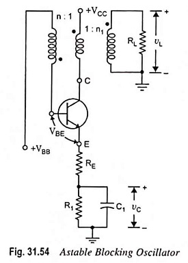
Assume initially, that there is a voltage vC on capacitor C1 larger than VBB – Vγ where Vγ is the cutin base-to-emitter voltage. Hence the transistor is off and the capacitor C1 discharges exponentially towards ground with a time constant R1C1. When vC becomes equal to VBB – Vγ, the base current starts to flow and the transistor comes out of cutoff. The flow of current through collector further lowers the collector voltage and through inductive coupling of pulse transformer increases the base voltage. This further increases the base current and hence the collector current. This regenerative action (for loop gain exceeding unity) quickly brings the transistor in saturation.
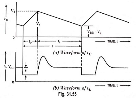
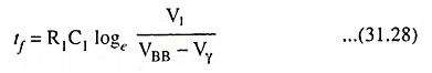
The pulse is generated and during the pulse duration tp, the capacitor C1 is recharged and attains a voltage V1, which is larger than the value it had at the beginning of the pulse (Fig. 31.55). The transistor comes out of saturation and the regenerative action brings it in the cutoff. The transistor now remains off for a time tf during which capacitor C1 discharges to the voltage at which transistor Q again enters its active region. At this point the cycle repeats itself. From Fig. 31.55 (a)
The period of the free running oscillations is T = tp + tf
The waveforms of vC (voltage across the R1C1 combination) and the vL (output voltage) are shown in Figs. 31.55 (a) and 31.55 (b) respectively. The overshoot is for the reasons discussed in monostable blocking oscillator.