Power Diode – Structure, Symbol, Characteristics and Types:
Diodes find many applications in electronics and electrical engineering circuits. Power diodes play a significant role in power electronics for conversion of electric power. A diode acts as a switch to perform various functions, such as switching in rectifiers, freewheeling in switching regulators, charge reversal of capacitor and energy transfer between components, voltage isolation, energy feedback from load to the power source, and trapped energy recovery.
Power diodes can be assumed as ideal switches for most applications but practical diodes differ from the ideal characteristics and have certain limitations. The power diodes are similar to P-N junction signal or low-power diodes. However, the power diodes have large power-, voltage-, and current-handling capabilities than those of ordinary diodes. The frequency response (or switching speed) is low in comparison to that of ordinary diodes.
Power diodes are of three types: General purpose, high speed (or fast-recovery), and Schottky. General-purpose diodes are available up to 6000 V, 4500 A, and the rating of fast-recovery diodes can go up to 6000 V, 1100 A. The reverse recovery time varies between 0.1 and 5 μs. The fast-recovery diodes are essentially required for high-frequency switching of power converters. Schottky diodes have low on-state voltage and very small recovery time, typically nanoseconds. The leakage current increases with the voltage rating and their ratings are limited to 100 V, 300 A. A diode conducts when its anode voltage is higher than that of the cathode; and the forward voltage drop of a power diode is very small, typically 0.5 and 1.2 V.
Basic Structure:
The structure of power diode is slightly more complex than that of a signal diode. In a power diode a lightly doped N– expitaxial layer is grown on an heavily doped N+ substrate. The P-N junction is developed by alloying N– layer with heavily doped P+ region as shown in Fig. 8.51. The N– layer in the figure is termed as drift region which is not the part of the signal diodes. The function of drift region is to absorb depletion layer of the reversed biased P+ N– junction J1. The width of this region determines the reverse voltage that can be applied across the device under safe operation. The drawback of N– layer is to add significant ohmic resistance to the diode when it is conducting in forward mode. This leads to large power dissipation in the diode, requiring proper cooling arrangements in large rating diodes.
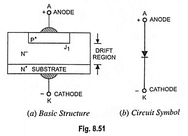
The circuit symbol of a power diode is the same as that for a signal diode [Fig. 8.51(b)].
The modifications in the context of diode, explained above, make them appropriate for high-power applications. As diode, or P-N junction, is the basic building block of all other power semiconductor devices; same basic modifications are required to be made in all low-power semiconductor devices; in the order to enhance their power-handling capabilities.
Diode Characteristics:
When the anode is positive w.r.t. cathode, the diode is said to be forward biased and the diode conducts. A conducting diode has a relatively small forward voltage drop across it; and the magnitude of this voltage drop depends on the manufacturing process and junction temperature. When the cathode is positive w.r.t. anode, the diode is said to be reverse biased. Under reverse-biased conditions, a small reverse current, called the leakage current, (in the range of micro- or milli-amperes) flows and this leakage current increases slowly in magnitude with the reverse voltage until the avalanche or zener voltage is reached.
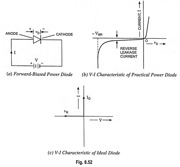
A forward biased diode is shown in Fig. 8.52 (a) . The volt-ampere characteristics of a diode are shown in Fig. 8.52 (b). For most practical purposes, a diode can be considered as an ideal switch, whose characteristics are shown in Fig. 8.52 (c).
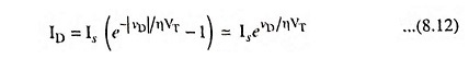
The V-I characteristics depicted in Fig. 8.52 (b) can be expressed by an equation, known as Shockley diode equation, and it is given under dc steady-state operation by
![]()
where vD is diode voltage with anode positive w.r.t. to cathode, Is is the leakage or reverse saturation current, typically in the range 10-6 to 10-15 A and η is empirical constant known as emission coefficient, or ideality factor.
The value of η depends on the material and the physical construction of the diode. For germanium diodes, η is taken to be 1 while for silicon diodes, the predicted value is 2. For most practical silicon diodes, the value of η lies in the range 1.1. to 1.8.
VT is the volt-equivalent of temperature (or thermal voltage) and is defined as
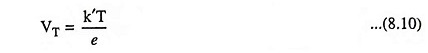
where k’ is Boltzmann’s constant (1.38 x 10⁻²³ J/K), T is absolute temperature in Kelvin and e is electron charge (1.602 x 10⁻¹⁹ coulomb).
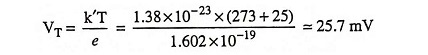
At a junction temperature of 25 °C, Eq. (8.10) gives
At a specified temperature, the leakage current Is is a constant for a given diode. The diode characteristic depicted in Fig. 8.52 (b) can be divided into three regions :

In the forward-biased region (vD > 0), the diode current ID is very small when the diode voltage vD is less than a specific value, known as threshold voltage, cut-in voltage, or turn-on voltage. Beyond cut-in voltage, the diode current rises rapidly and the diode is said to be conducting. For silicon diode, the cut-in voltage is around 0.7 V. In the conducting state of diode, the forward voltage drop is of the order of 0.8 to 1 V.
The V-I characteristics of power diode are similar to those of signal diode with the exception that the current in power diodes varies linearly rather than exponentially with voltage. The high magnitude of current in a power diode leads to ohmic drop that hides the exponential part of V-I curve. The N– region, or drift region, forms a considerable drop in the ohmic resistance of power diodes.
For vD > 0.1 V, which is usually the case, ID ≫ Is and Eq. (8.9) can be approximated within 2.1% error to
![]()
In the reverse-biased region, when vD is negative (vD < O), and |vD| ≫ VT which occurs for vD < – 0.1 V, the exponential term of Eq. (8.9) becomes negligibly small compared with unity and the diode current becomes
which indicates that the diode current ID is in the reverse direction and is constant and is equal to Is.
In the breakdown region, the reverse voltage is high, usually exceeding 1,000 V. The magnitude of reverse voltage may exceed a specified voltage, called the breakdown voltage VBR. With a small change in reverse voltage beyond VBR, the reverse current increases rapidly. The operation in the breakdown region will not be destructive, provided that the power dissipation is within a “safe limit” that is specified in the manufacturer’s data sheet. However, it is often necessary to limit the reverse current in the breakdown region to restrict the power dissipation within a permissible value.
Diode manufacturers also indicate the value of peak inverse voltage (PIV) of a diode. It is the maximum reverse voltage that can be applied to the diode during its working.
The power diodes are now available with forward current rating of 1 A to several thousand amperes and with reverse voltage rating of 50 V to 5,000 V or more.
Diode Reverse Recovery Characteristics:
The current in a forward-biased junction diode is due to the net effect of majority and minority carriers. Once a diode is in a forward conducting state and then its forward current is reduced to zero (due to the natural behavior of the diode circuit or by applying a reverse voltage), the diode continues to conduct due to minority carriers that remain stored in the P-N junction and the bulk semiconductor material. The minority carriers require a certain time to recombine with opposite charges and to be neutralized. This time is called the reverse recovery time of the diode.
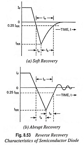
Figure 8.53 depicts two reverse recovery characteristics of junction diodes viz. soft-recovery type and abrupt recovery type. The soft-recovery type is more common. The reverse recovery time trr is defined as the time between the instant forward current becomes zero and the instant reverse recovery current decays to 25% of its reverse peak value IRR as shown in Fig. 8.53. The reverse recovery time trr is composed of two segments of time ta and tb. The time ta is the time between zero crossing of forward current and peak reverse current IRR. During the time interval of ta, charge stored in the depletion region is removed. Time tb is measured from the instant of reverse peak value IRR to the instant when 0.25 IRR is reached. During this interval of time charge is removed from the semiconductor layers. The ratio tb/ta is known as softness factor (SF). For practical purposes, we are concerned with the total recovery time and the peak value of the reverse current IRR
![]()
The peak reverse current can be expressed as
![]()
where di/dt is the rate of change of reverse current.
The reverse recovery time trr depends on the junction temperature, rate of decrease of forward current, and the forward current prior to commutation, IF.
The reverse recovery charge QRR is the amount of charge which flows through the diode in the reverse direction due to change over from forward conducting state to reverse blocking state. The value of QRR can be found from the area enclosed by the path of reverse recovery current. This enclosed area is shown in Fig. 8.53 and can be assumed to be triangular. Therefore
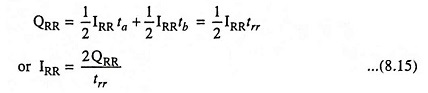
From Eqs. (8.14) and (8.15)
![]()
If tb is negligible as compared to ta (as in the case of abrupt recovery), then trr ≈ ta. Then
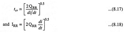
It is seen that reverse recovery time trr and peak reverse current IRR depend on stored charge QRR and rate of change of current di/dt. The stored charge QRR depends on forward anode current IF.
Since the reverse recovery time depends on QRR (which depends on forward current IF), this time can be reduced by keeping the current IF at a low value. In fast recovery diodes for voltage ratings above 400 V, trr is reduced by gold or platinum diffusion. For voltage ratings below 400 V epitaxial diodes having narrow base width provide fast recovery and reverse recovery time of less than 50 ns.
Types of Power Diodes:
Ideally, a diode should have no reverse recovery time. However, the manufacturing cost of such a diode may increase. In many applications, the effects of reverse recovery time is not significant, and cheaper diodes can be used. Depending on the recovery characteristics and manufacturing techniques, the power diodes may be classified as (i) Standard or general purpose diodes (ii) Fast-recovery diodes (iii) Schottky diodes.
The characteristics and practical limitations of these types restrict their applications.
1. General Purpose Diodes. These diodes have relatively high reverse recovery time, typically 25 μs; and are employed in low-speed applications, where recovery time is not critical (e.g., diode rectifiers and converters for a low-input frequency up to 1kHz applications and line-commutated converters). Their ratings cover a very wide range from less than 1 A to several thousands of amperes with voltage rating from 50 V to around 5 kV. These diodes are generally manufactured by diffusion process. However, alloyed types of rectifiers, used in welding power supplies, are most cost effective and rugged, and their ratings can go up to 1500 V, 400 A.
2. Fast-Recovery Diodes. As the name indicates their recovery time is very low, generally less than 5 μs. Their current ratings are from about 1 A to several thousands of amperes and voltage ratings from about 50 V to about 3 kV. For high voltage ratings (more than 400 V), they are manufactured by diffusion process and the recovery time is controlled by platinum or gold diffusion. For less than 400 V rating epitaxial diodes provide very fast recovery time. Epitaxial diodes have a very narrow base width resulting in recovery times of about 50 ns.
Power Diode Ratings:
1. Voltage Rating. Power diodes have two voltage ratings viz., repetitive peak inverse voltage (VRRM) and non-repetitive peak inverse voltage (VRM). The non-repetitive peak inverse voltage determines the capability of the diode to withstand a reverse voltage which may occur occasionally. On the other hand, repetitive peak inverse voltage is applied across a diode in every cycle.
2. Current Ratings. Current rating in every device is based on its capacity to dissipate heat so that the temperature does not rise beyond permissible limit. In all semiconductor devices the current rating is determined by the allowable junction temperature. Power diodes have three current ratings, i.e., average current, rms current and peak current. Actual value of each of these currents must be below the rated value. For any given current waveshape the actual values of average, rms and peak current can be found either by measurement or calculation.