Shockley Diode Equation, Symbol, Operation and Applications:
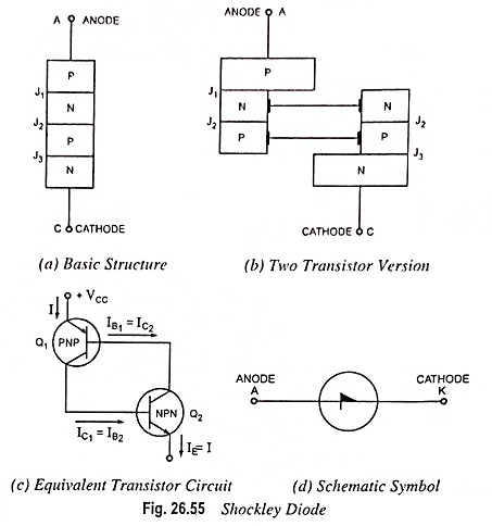
The four layer diode, also called the Shockley diode after its inventor Willian Shockley, is essentially a low-current SCR without a gate. It is classified as a diode because it has only two external terminals viz. anode and cathode. Because of its four doped regions, it is often called a P-N-P-N diode. The basic structure, two transistor version, equivalent transistor circuit and schematic symbol of a Shockley diode are shown in Fig. 26.55.
Shockley Diode Working:
The easiest way to understand how it operates is to visualize it to be formed of two transistors Q1 and Q2 placed back to back, as shown in Fig. 26.55 (b). Figure 26.55 shows the diode split-up into two parts, displaced mechanically but connected electrically. The left half is a P-N-P transistor while the right half is an N-P-N transistor. It may be seen that N-type base region of P-N-P transistor forms the collector of N-P-N transistor while P-type base of N-P-N transistor forms the collector of P-N-P transistor. Thus the four layer diode is equivalent to the latch shown in Fig. 26.55.
Collector currents IC1 and IC2 for transistors Q1 and Q2 are indicated. In the active region the collector current is given by
![]()
where IE is the emitter current, ICO is the reverse saturation current, and α is the short-circuit common-base forward current gain.
Applying above Eq. (26.22), in turn, to transistors Q1 and Q2 we have

But the sum of currents IC1 and IC2 is equal to the total current through the device i.e.,
![]()
Solving above equations we have
From above Eq. (26.25) it is obvious that the current I through the device is small (approximately the sum of collector saturation currents of the two equivalent transistors) as long as the sum (α1 + α2) is small as compared to unity. It seems that the current I increases rapidly when the sum (α1 + α2) approaches unity. The current does not increase beyond limit as Eq. (26.25) implies, however, because the derivation is no longer valid as (α1 + α2) approaches unity. Since junction J2 becomes forward biased in the forward conducting state, both transistors become saturated after switching. The two transistors remain in saturation while the device is in the forward conducting state, being held in saturation by the device current.
Because there are no trigger inputs, the only way to switch the device on is to increase the anode-to-cathode voltage VAK to the forward switching voltage, and the only way to open it is by low-current drop out. With a four layer diode it is not necessary to reduce the current all the way to zero to open the latch. The internal transistors of the device will come out of saturation when the current is reduced to a low value, called the holding current. The forward switching voltage Vs is equivalent of the SCR forward breakover voltage, and the minimum current at which device will switch on is the switching current Is.
Shockley Diode Characteristics:
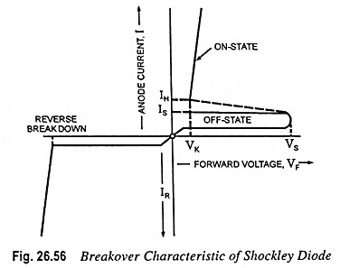
Voltage-current characteristic of a Shockley diode is shown in Fig. 26.56. The device has two operating states: conducting and nonconducting. In nonconducting state, it operates on lower line with negligible current and a voltage less than switching voltage or breakover voltage. When the voltage tries to exceed the breakover voltage, the device breaks down and switches along the dotted line to the conducting or on-state. The dotted line indicates an unstable or a temporary condition. The device can have current and voltage values on this dotted line only briefly as it switches between the two stable operating states. In conducting state or in on-state, the device operates on the upper line. As long as the current through the device is greater than the holding current IH, then the voltage across it is slightly greater than knee voltage, VK. When the current falls below the level of the holding current IH, the device switches back along the dotted line to the nonconducting or off-state.
Shockley Diode Application:
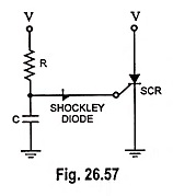
One common application of the Shockley diode is as a trigger switch for an SCR. The circuit is shown in Fig. 26.57. When the circuit is energized, the capacitor will start getting charged and eventually, the voltage across the capacitor will be sufficiently high to first turn on Shockley diode and then the SCR.
Another application of this diode is as a relaxation oscillator.