Complementary Metal Oxide Semiconductor (CMOS):
With active load switching, the current drain with a low output is approximately equal to ID(sat). This may cause a problem with battery operated equipment. One way to reduce the current drain of a digital circuit is with complementary MOS (CMOS). Complementary metal oxide semiconductor devices are chips in which both P-channel and N-channel enhancement MOSFETs are connected in push-pull arrangement. The basic connections for Complementary Metal Oxide Semiconductor are shown in Fig. 13.97(a) and Fig. 13.97(b).
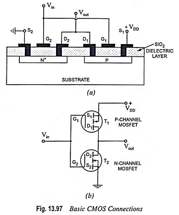
In this circuit, two MOSFETs (P-channel MOSFET and N-channel MOSFET) are connected in series so that source of P-channel device is connected to a positive voltage supply +VDD and the source of N-channel device is connected to the ground. Gates of both the devices are connected as a common input and drain terminals of both the devices are connected together as a common output.
When the input is kept low i.e., at 0 volt, then gate of MOSFET T1 is at negative potential w.r.t. the source S1. So MOSFET T1 will be ON with its resistance RON = 1 kΩ, while gate of MOSFET T2 will be at 0 volt relative to its source. So T2 will be OFF with its resistance ROFF = 1010 Ω. Both of these resistances act like a potential divider and output of this will be approximately +VDD volts.
In other case when the input is kept at high level i.e., +VDD volts then the gate of MOSFET T1 is at zero potential relative to the source, so T1 will be OFF with its resistance ROFF = 1010 Ω while gate of MOSFET T2 will be at positive potential relative to its source so the MOSFET T2 will be ON with its resistance RON = 1 kΩ. In this case output will be approximately 0 volt.
Except for a short time as the voltage drop from +VDD to zero or rises from zero to +VDD, the series combination of P-channel MOSFET (or PMOS) and N-channel MOSFET (or NMOS) has one transistor off with no current then drawn from the power supply. Thus the Complementary Metal Oxide Semiconductor circuit operates with the input either high or low while drawing no power from the supply except during the brief time while switching between high and low output levels, when both transistors are ON as one is turning ON and the other is turning OFF. In fact, the power consumption of a CMOS circuit is 0 at dc conditions, increasing as the applied signal frequency increases since the circuit is switching more often.
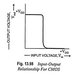
The Complementary Metal Oxide Semiconductor device is used primarily in digital circuits, operating to provide output of either 0 V or + VDD (+5 V) while drawing very little power from the supply. Most low-power ICs (integrated circuits) are built using CMOS transistors. Curve shown in Fig. 13.98 gives relation between input and output voltages.
The main advantage of CMOS is that the power dissipation is very small typically 50 nW.
CMOS Handling:
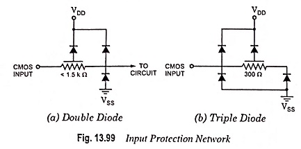
All MOS devices have insulated gates that are subject to voltage breakdown. For instance the gate oxide for Motorola CMOS devices is about 900 Å thick and breaksdown at a gate-source potential of about 100 V. To guard against such a breakdown from static discharge or other voltage transient, the protection networks shown in Figure 13.99 (a), 13.99 (b) are used on each input to the CMOS device.
Static damaged devices behave in different ways, depending on the severity of the damage. The most severely damaged inputs are the easiest to detect because the input has been completely destroyed and is either shorted to VDD, shorted to VSS or open-circuited. The effect is that the device no longer responds to signals present at damaged input. Less severe cases are more difficult to detect because they indicate as intermittent failures or as degraded performance. Another effect of static damage is that the inputs generally have increased leakage currents.
Although the input protection network provides a great deal of protection, CMOS devices are not immune to large static voltage discharges that can be generated during handling. For example, static voltage generated by a person walking over a waxed floor have been measured in the 4-15 kV range (depending upon humidity, surface conditions etc.).
So following are the some of the important precautions that are to be observed.
1. Do not exceed the maximum ratings specified in the data sheet.
2. All unused device inputs should be connected to VDD or VSS.
3. All low-impedance equipment’s (pulse generators, etc) should be connected to CMOS inputs only after the device is energized. Similarly, this type of equipment should be disconnected before power is switched off.
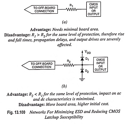
4. Circuit boards containing Complementary Metal Oxide Semiconductor devices are merely extensions of the devices, and the same handling precautions apply. Contacting edge connectors wired directly to device inputs can cause damage. Plastic wrapping should be avoided. While external connections to a PC board are connected to an input of CMOS device, a resistor should be used in series with the input. This series resistor helps limit accidental damage if the PC board is removed and brought into contact with static generating materials. The limiting factor for the series resistor is the added delay. This is caused by the time constant formed by the series resistor and input capacitance. Note that the maximum input rise and fall times should not be exceeded. In Fig. 13.100 two possible networks are shown using a series resistor to reduce ESD (electrostatic discharge) damage.
These networks are useful for the protection of (i) digital inputs and outputs (ii) analog inputs and outputs (iii) 3-state outputs (iv) bidirectional (I/O) ports.
5. All CMOS devices should be stored or transported in materials that are antistatic. CMOS devices must not be inserted into conventional plastic ‘snow’, styrofoam, or plastic trays, but should be left in their original container until ready for use.
6. All Complementary Metal Oxide Semiconductor devices should be placed on a ground bench surface and operators should ground themselves prior to handling devices, since a worker can be statically charged w.r.t the bench surface. Wrist straps in contact with skin are strongly recommended.
7. Nylon or other static generating materials should not come in contact with CMOS devices.
8. If automatic handlers are being used, high levels of static electricity may be generated by the movement of the device, the belts or the boards. Reduce static build-up by using ionized air blowers or room humidifiers. All parts of the machines which come into contact with the top, bottom, or sides of IC packages must be grounded to metal or other conductive material.
9. Cold chambers employing CO2 for cooling should be equipped with baffles, and the CMOS devices must be contained on or in conductive material.
10. When lead-straightening or hand soldering is required, provide ground straps for the apparatus used and be sure that soldering ties are grounded.
11. The use of static detection meters for production line surveillance is highly recommended.
12. Equipment specifications should alert users to the presence of CMOS devices and require familiarization with this specification prior to performing any kind of maintenance or replacement of devices or modules.
13. Do not insert or remove CMOS devices from test sockets with power applied. Check all power supplies to be used for testing devices to be certain there are no voltage transient present.
14. Double check test equipment setup for proper polarity of VDD and VSS before conducting parametric or functional testing.
15. Do not recycle shipping rails or trays. Repeated use cause deterioration of their antistatic coating.