CMOS NAND Gate Circuit Diagram:
Fig. 3.3 shows CMOS NAND Gate Circuit Diagram 2-input NAND gate. It consists of two P-channel MOSFETs, Q1 and Q2, connected in parallel and two N-channel MOSFETs, Q3 and Q4 connected in series.
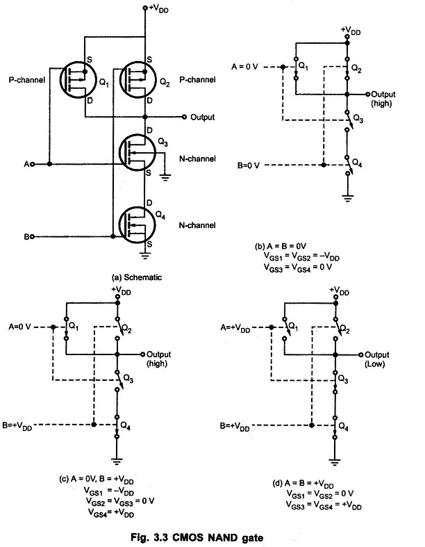
P-channel MOSFET is ON when its gate voltage is negative with respect to its source whereas N-channel MOSFET is ON when its gate voltage is positive with respect to its source
Fig. 3.3 (a) shows the equivalent switching circuit when both inputs are low. Here, the gates of both P-channel MOSFETs are negative with respect to their sources, since the sources are connected to +VDD. Thus, Q1 and Q2 are both ON. Since the gate – to – source voltages of Q3 and Q4 (N-channel MOSFETs) are both 0V, those MOSFETs are OFF. The output is therefore connected to +VDD (HIGH) through Q1 and Q2 and is disconnected from ground, as shown in the Fig. 3.3 (b).
Fig. 3.3 (c) shows the equivalent switching circuit when A = 0 and B = +VDD. In this case, Q1 is on because VGS1 = −VDD and Q4 is ON because VGS4 = +VDD. MOSFETs Q2 and Q3 are off because their gate-to-source voltages are 0 V. Since Q1 is ON and Q3 is OFF, the output is connected to +VDD and it is disconnected from ground. When A = +VDD and B = 0V, the situation is similar (not shown) ; the output is connected to +VDD through Q2 and it is disconnected from ground because Q4 is OFF. Finally, when both inputs are high (A = B = +VDD), MOSFETs Q1 and Q2 are both OFF and Q3 and Q4 are both ON. Thus, the output is connected to the ground through Q3 and Q4 and it is disconnected from +VDD.
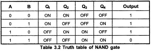
The Table 3.2 summarizes the operation of 2-input CMOS Inverter NAND gate.