Common Gate Circuit:
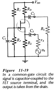
The FET Common Gate Circuit (CG) shown in Fig. 11-19 uses voltage divider bias. The ac output is taken from the drain terminal, and an external load (RL) is capacitor-coupled to the drain, exactly as in the case of a common-source circuit. Unlike a CS circuit, the ac input for the CG circuit is applied to the FET source terminal (via C3), and a capacitor (C1) is included to ac short-circuit the gate to ground. Because the gate is grounded, all of the ac input voltage appears across the gate-source terminals.
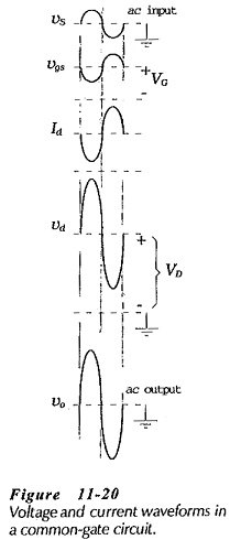
The current and voltage wave forms for the CG circuit shown in Fig. 11-20 illustrate the circuit operation. When the instantaneous level of the ac signal voltage increases, the source voltage increases while the gate voltage remains constant. Consequently, the gate-source voltage decreases, the drain current is reduced, and the output voltage at the drain terminal is increased. Similarly, when vi decreases, vgs increases, Id increases, and vd decreases. Thus, an increase in vi causes an increase in vo, and a decrease in vi produces a decrease in vo, so, there is no phase shift between the input and the output. (See the voltage and current waveforms in Fig. 11-20.)
Common Gate Equivalent Circuit:
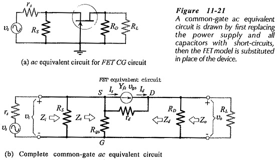
As in the case of other circuits, the supply voltage and capacitors in Fig. 11-19 are replaced with short-circuits in order to study the circuit ac performance. This gives the common-gate ac equivalent circuit in Fig. 11-21(a). The input terminals of the ac equivalent circuit are seen to be the PET source and gate, and the output terminals are the drain and gate. The gate terminal is common to both input and output, so the circuit is named common-gate.
The completer CG ac equivalent circuit is drawn by substituting the FET model into the ac equivalent circuit, [Fig. 11-21(b)]. As always, the indicated current directions and voltage polarities are those that are produced by a positive-going signal voltage.
Input Impedance:
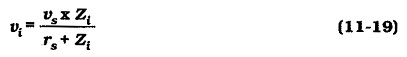
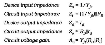
Looking into the source and gate terminals of the CG circuit in Fig. 11-21(b), is similar to ‘looking into’ the output of a common-drain circuit. Therefore, the equation for the Common Gate Circuit device input impedance (Zs) is derived in the same way as, the equation for Zs in the common-drain circuit.
![]()
The circuit input impedance is Rs in parallel with the device input impedance.
![]()
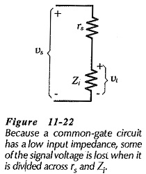
Using a typical Yfs of 5000 μS, the input impedance of a Common Gate Circuit is around 200 Ω. Low input impedance is the major disadvantage of the Common Gate Circuit, because the signal voltage is divided across rs and Zs, (see Fig. 11-22).
Output Impedance:
The output of a Common Gate Circuit is taken from the drain terminal, as in the case of a common-source circuit. So, the common-gate output impedance is the same as the common-drain output impedance. At the drain terminal,
![]()
and the circuit output impedance is,
![]()
Voltage Gain:
From Fig. 11-21(b),
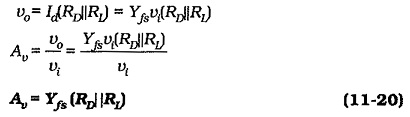
Equation 11-20 is similar to Eq. 11-7 for the voltage gain of a common-source circuit, with the exception that there is no minus sign in Eq. 11-20. So, the voltage gain for a Common Gate Circuit is the same as the voltage gain for a common-source circuit with the same component values. As, already discussed, there is no phase shift between the input and output of a Common Gate Circuit, hence the absence of the minus sign in Eq. 11-20.
Effect of Unbypassed Gate Resistors:
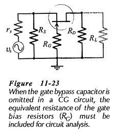
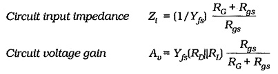
If capacitor C1 is not present in the CG circuit in Fig. 11-19, the FET gate is not ac short-circuited to ground. So, a resistance (RG = R1||R2) must be included in the ac equivalent circuit (see Fig. 11-23), and in the complete CG ac equivalent circuit. The presence of the unbypassed gate resistors affects the circuit input impedance and voltage gain. Analysis of the equivalent circuit shows that,
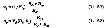
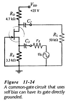
When Rgs ≫ RG (which is usually the case), Eq. 11-21 gives Zi = 1/Yfs, and Eq 11-22 gives Av= Yfs(RD||RL), which are the equations for a CG circuit with the gate bypassed to ground The Zi and Av effects occur only in situations where very high value bias resistors are used in a CG circuit. Figure 11-24 shows a CG circuit that uses self bias. In this case, RG is omitted because there is no signal applied at the gate input; the gate is directly grounded and no gate bypass capacitor is required.
Summary of CG Circuit Performance:
With the gate bypassed to ground:
With the gate unbypassed:
A Common Gate Circuit has a voltage gain, no phase shift between input and output, low input impedance, and relatively high output impedance.