Common Source JFET Amplifier with AC Equivalent Circuit:
The Common Source JFET Amplifier Circuit configuration is the most widely employed configuration. It is because this configuration provides high input impedance, good voltage gain and moderate output impedance.
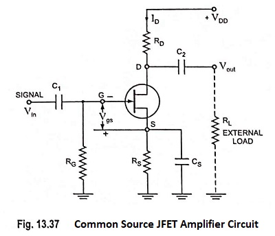
The circuit of a common source N-channel JFET amplifier using self bias is shown in Fig. 13.37. The signal source, Vin is connected to JFET gate through coupling capacitor C1 and external load RL is connected to the drain terminal D via coupling capacitor C2. RG is used to provide leakage path to the gate current, RS for developing gate bias and CS for providing ac ground to the input signal.
Note that the polarity of the capacitors in Fig. 13.37—the negative terminal of each (polarized) capacitor must always be at a lower dc potential than the positive terminal. Incorrectly connected capacitors can affect the bias conditions and ac performance of the circuit.
For ac considerations, bypass capacitor CS effectively ties the FET source terminal to the ground level. Thus, all of the input voltage Vin is developed across the gate source terminals. With the increase or decrease in input voltage, gate-source voltage Vgs changes and corresponding change in Vgs makes the drain current ID to increase or decrease correspondingly.
The phase relationship between the circuit input and output voltages can be determined by considering the effect of a positive going input signal. When input voltage Vin increases in positive direction, it reduces the negative gate-source voltage, –Vgs. The reduction in –Vgs raises the level of drain current ID and consequently increases the voltage drop across drain resistance RD.
Since VD = VDD – IDRD, the increase in ID results in a drop in drain (output) voltage VD. Thus as Vin increases in a positive direction, Vout goes in a negative direction. Similarly when Vin goes negative, the resultant increase in –Vgs reduces the drain current ID which, in turn, reduces the voltage drop across RD and develops a positive going output voltage Vout. Thus, the amplifier output voltage is 180° out of phase with the input voltage.
Analysis: The first step in ac analysis of the common source circuit is to draw the ac equivalent circuit. This is done by replacing all the capacitors with short circuits and reducing dc supply voltages to zero. AC equivalent circuit for Common Source JFET Amplifier is given in Fig. 13.38.
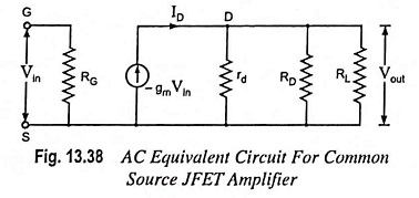
Input Resistance: In an ideal JFET Rgs is infinite because IG = 0. However, in actual device Rgs is not infinite but extremely high (100 MΩ or so) in comparison to RG. Thus, input resistance
![]()
Output Resistance: Looking into the drain and source terminals, the large drain resistance rd is seen. Thus,
![]()
Zd is the device output impedance; the circuit output impedance is RD in parallel with Zd, so
![]()
Since usually rd ≫ RD, the circuit output impedance is taken to be RD.
Voltage Gain:
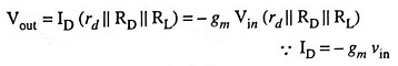
Output voltage,
and voltage gain,
usually rd ≫ RD || RL
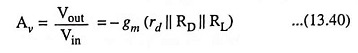
So voltage gain,
![]()
The minus sign indicates that output voltage Vout is 180° out of phase with input voltage Vin.