Gate Bias Circuit:
Circuit Operation – Consider the Gate Bias Circuit shown in Fig. 10-6. The FET gate terminal is connected via resistor RG to a bias voltage VG. If the gate is directly connected to the bias source (instead of using RG), any ac signal applied to the gate would be short-circuited to VG.
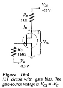
There is no gate current to produce a voltage drop across RG so the gate-source voltage remains constant at VG. Depending on the device transfer characteristics, VG sets the level of ID in the FET.
The ID level can be readily determined, if the transfer characteristic is available for the particular FET used in the circuit. If the device is replaced, ID is determined by the transfer characteristic of the new device. Like the base current in a BJT base bias circuit, the FET gate voltage does not change when the device characteristics change.
Circuit Analysis:
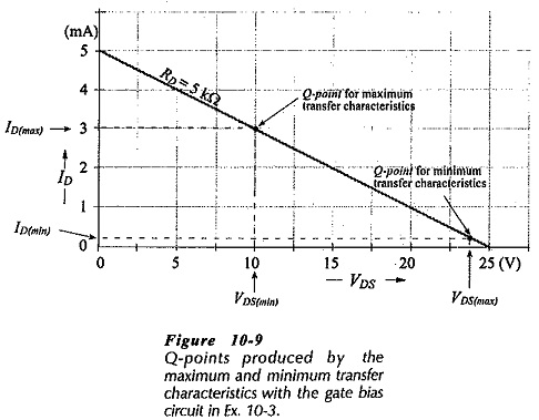
As discussed already, each FET of a given type number has maximum and minimum transfer characteristics, and these must be employed to determine the maximum and minimum possible levels of ID in the circuit. A Gate Bias Circuit is most easily analyzed by drawing a bias line vertically on the transfer characteristics from VGS = -VG. The levels of ID(min) and ID(max) are read from the intersections of the bias line with the transfer characteristics, and the maximum and minimum drain-source voltages can then be calculated using these ID levels.
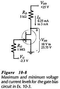
The maximum and minimum ID and VDS levels determined are illustrated by the circuit current and voltage levels in Fig. 10-8, and by the Q-points plotted in Fig. 10-9. As already discussed, JFETs with a given type number have a wide range of transfer characteristics, so
PET maximum and minimum transfer characteristics should always be used for practical circuit analysis.
The gate bias technique produces a wide range of ID and VDS levels for any FET with a particular type number. It is possible to adjust VG to set VDS to a desired voltage. However, this is normally done only in an experimental situation. Slightly more complicated bias circuit must be employed for more predictable voltage and current conditions.
Analysis of a Gate Bias Circuit can be performed without drawing the FET transfer characteristics.
Gate Bias for a p-channel JFET:
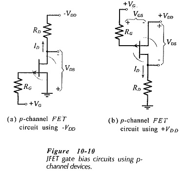
A gate bias circuit using a p-channel JFET is shown in Fig. 10-10(a). This is similar to n-channel JFET Gate Bias Circuit except that VDD is a negative voltage and VG is a positive quantity. Figure 10-10(b) shows the same p-channel JFET circuit with a positive supply voltage. In this case, the FET source terminal is connected to VDD, and RD is connected to ground. To reverse bias the gate channel junctions, the gate terminal must be positive with respect to the source. So, gate bias voltage VG must be positive with respect to VDD, as illustrated. The p-channel gate bias circuit can be analyzed in exactly the same way as an n-channel circuit.