Bias Circuit Design:
Bias Circuit Design can be amazingly simple. Usually, it is just a matter of determining the required voltage across each resistor and the appropriate current levels. Then, the resistor values are calculated by application of Ohm’s law.
Designs usually begin with specification of the supply voltage and the required levels of IC and VCE. The resistor values are calculated to meet these requirements, and standard value resistors are selected. Usually, resistors with a tolerance of ±10% are used wherever possible. These are less expensive than ±5% and ±1% components.
Base Bias Circuit Design:
A base bias circuit is very easily designed. This is illustrated in Fig. 5-36.
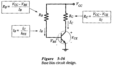
When selecting the standard value resistors, a decision must be made whether to select the next smaller resistance value or the next larger value. In general, it is best to select the resistance value that tends to increase the transistor collector-emitter voltage, thus keeping VCE from approaching zero.
After design, the circuit should be analysed using the selected standard-value components and the maximum and minimum hFE values for the transistor.
Collector-to-Base Bias Circuit Design:
The design procedure for a collector-to-base bias circuit is similar to that for base bias, with the exception that the voltage and current levels are different for calculating RB and RC. In collector-to-base bias, the voltage across RB is (VC – VBE) and the current through RC is (IB + IC). The design equations are shown in Fig. 5-38.
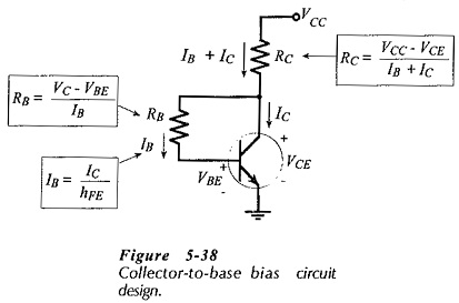
Once again decisions must be made about selecting the next larger or the next smaller standard value resistors. As in the case of the base bias circuit , selection of the smaller value for RC and the larger value for RB tends to produce a larger VCE than the specified level. The design should be analysed using the selected standard-value components and the transistor hFE(max) and hFE(min) values.
Voltage Divider Bias Circuit Design:
When designing a voltage divider bias circuit the voltage divider current (I2 in Fig. 5-40) should be selected much larger than the transistor base current (IB). This makes the base voltage (VB) a stable quantity largely unaffected by the transistor hFE value. However, a high level of I2 results in small resistance values for R1 and R2, and this gives the circuit an undesirable low input impedance.
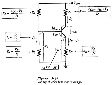
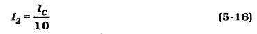
A rule-of-thumb approach to selection of I2 is to use a voltage divider current approximately equal to one-tenth of the transistor collector current.
As can be easily demonstrated, this gives reasonably large values for R1 and R2 while still keeping I2 much larger than IB.
If VE is not specified, it should be selected much larger than the transistor VBE.![]()
This is because VBE can vary from transistor to transistor, and it can also change with temperature increase or decrease. Making VE very much larger than VBE minimizes the effect of VBE changes on the circuit bias conditions. Typically, as another rule-of-thumb, VE is selected as 5 V regardless of the supply voltage. When VCC is low, VE can be as low as 3 V.
Figure 5-40 shows the equations used for calculating each resistor value.
Designing with Standard Resistor Values:
In all circuit designs a suitable standard resistor should normally be selected when each resistor value is calculated, instead of first completing the design. Then, the new resistor voltage drop or current level should be determined before calculating the next component value.
More Bias Circuits:
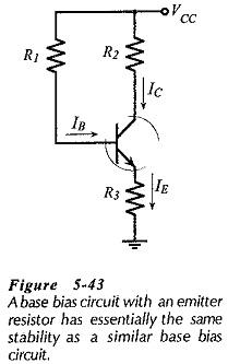
Base Bias with Emitter Resistor:
The bias circuit shown in Fig. 5-43 is the usual base bias arrangement with the addition of an emitter resistor. Analysis reveals that this circuit has essentially the same stability characteristics as a similar base bias circuit. The only advantage of the emitter resistor in this case is that it gives the circuit a higher input resistance. An emitter resistor could also be employed with collector-to-base bias, and this would also produce a higher input resistance without significantly altering the circuit stability.
Voltage Divider and Collector-to-Base Combination:
Figure 5-44 shows a voltage divider bias circuit with resistor R1 connected to the transistor collector instead of to the supply. Thus, the circuit combines collector-to-base bias with voltage divider bias. An analysis of the circuit shows that this combination produces even greater bias stability than voltage divider bias alone.
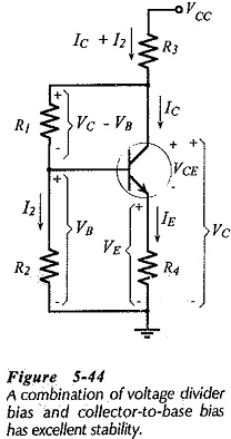
The design procedure for this circuit is similar to voltage divider bias design, except that for calculating the resistances of R1 and R3, the voltage across R1 is (VC – VB) instead of (VCC – VB), and the current through R3 is (IC + I2).
Emitter Current Bias:
The emitter current bias circuit in Fig. 5-46(a) uses a plus and minus voltage supply (+VCC and -VEE) and has the transistor base grounded via resistor R3. This is similar to voltage divider bias, in fact, as illustrated In Fig. 5-46(b), a voltage divider (R1 and R2) could be used to provide VB instead of grounding the base via R1.
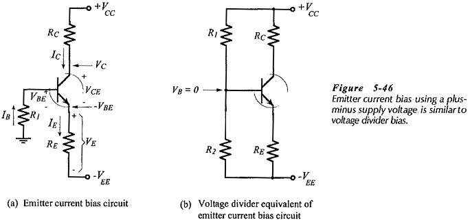
So long as there is very little voltage drop across base resistor R1, in Fig. 5-46(a), this circuit (like voltage divider bias), has excellent bias stability. Normally, R1 is selected to have a voltage drop much smaller than the transistor base-emitter voltage:
![]()
A reasonable rule-of-thumb to use is,
![]()
This mean that the transistor base voltage can be treated as ground level, and the voltage at the emitter terminal is always VBE below ground, [see Fig. 5-46(a)]. So, the voltage across RE is a constant quantity:
![]()
The transistor collector voltage is,
![]()
and, as illustrated, the collector-emitter voltage is
![]()