JFET Bias Circuit Troubleshooting:
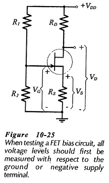
Voltage Measurement – JFET Bias Circuit Troubleshooting are similar to those for BJT bias circuits. The major difference is that there is only one junction in the FET (the gate-channel junction) that might become short-circuited or open-circuited. To determine if the circuit is functioning correctly, the FET terminal voltages should all be measured with respect to ground, as illustrated in Fig. 10-25. This is exactly as done for a BJT circuit, and, here again, if the voltage levels are not satisfactory, the circuit must be further investigated to locate the fault.
Common Errors:
Before proceeding further, the following list of common errors should be considered. These apply equally to FET and BJT circuits.
- Power supply not switched on.
- Power supply current limiter control incorrectly set.
- Cables incorrectly connected to the power supply.
- Volt-Ohm-Milliammeter (VOM) function incorrectly selected.
- Wrong VOM terminals used.
- Incorrect component connections.
- Incorrect resistor values.
- Resistors in the wrong places.
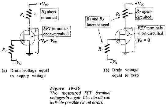
Gate Bias:
Figure 10-26 illustrates typical error sources in a gate bias circuit. Normally, the gate should be negative with respect to ground, and the drain voltage should be anywhere in the range of perhaps 3 V to (VDD – 2 V). If VD ≈ VDD, as in Fig. 10-26(a), the FET terminals might be open-circuited, or R2 might be shorted. When VC ≈ 0, as in Fig. 10-26(b), R1 and R2 might be interchanged (the high-value and low-value resistors in the wrong places). Other possibilities are that R2 is open-circuited, or the FET terminals are short-circuited.
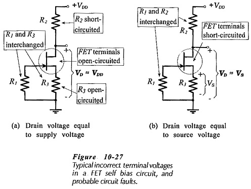
Self Bias:
Possible reasons for incorrect voltage levels in a self-bias circuit are illustrated in Fig. 10-27. These are similar to those discussed, for gate bias. If VD is approximately equal to VDD [Fig 10-27(a)], resistor R3 or one of the transistor terminals could to be open-circuited, or R1 and R3 might be interchanged. Alternatively, R2 might be short circuited. If VD equals VS [Fig 10-27(b)], the FET transistor terminals might be short-circuited, or R1 and R2 might be in the wrong places (interchanged).
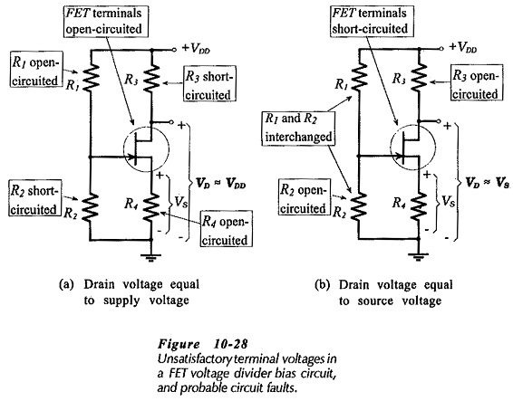
Voltage Divider Bias:
Unsatisfactory voltage measurements and probable errors in a voltage divider bias circuit are shown in Fig. 10-28. If VD equals VDD [Fig. 10-28(a)], R1 or R4 might be open-circuited. Alternatively, R2 or R3 might be short-circuited, or the FET terminals might be open-circuited. When VD approximately equals VS (Fig. 10-28(b)], R2 might be open-circuited, or R1 and R2 might be interchanged. Another possibility is that the FET terminals are short-circuited.