Basic JFET Biasing Circuits Comparison:
The Basic JFET Biasing Circuits Comparison (gate bias, self-bias, and voltage divider bias) are similar in performance to the three basic BLIP bias circuits, (base bias, collector-to-base bias, and voltage divider bias). Comparing the performance of FET bias circuits, it should be recalled that each FET type number has maximum and minimum transfer characteristics.
The particular transfer characteristic for each individual transistor is normally not known. Therefore, as already stated, the specified maximum and minimum transfer characteristics must be used when analyzing (or designing) a FET bias circuit.
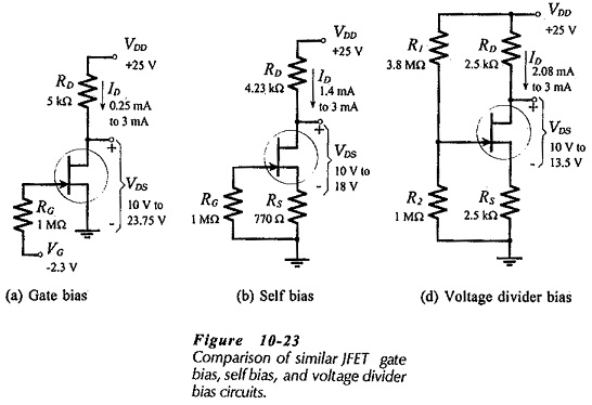
Consider the basic Basic JFET Biasing Circuits Comparison reproduced in Fig. 10-23. Each circuit uses a 25 V supply and a 5 kΩ (total) load resistance, and each uses a FET with the same maximum and minimum transfer characteristics. The circuits are analysed to determine the maximum and minimum ID and VDS levels. The calculated quantities are indicated on each circuit in Fig. 10-23, and the Q point ranges are illustrated in Fig. 10-24.
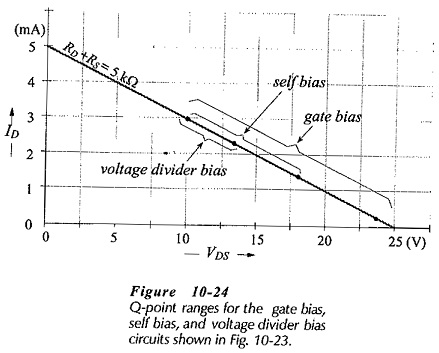
If the FET in the gate bias circuit fails and has to be replaced with another (same type number) device, the new VDS level could be anywhere from 10 V to 23.75 V. The self-bias circuit in the same circumstance (with the same FET type number) would have a VDS ranging from 10 V to 18 V when the FET is replaced. For the voltage divider bias circuit in this situation, the measurable VDS range with a new device would be 10 V to 13.5 V. Clearly, self-bias gives more predictable bias conditions than gate bias, and voltage divider bias gives the most predictable bias conditions. Because of its better performance, voltage divider bias is usually preferred.
Note that, for all three basic bias circuits in Fig. 10-23, the minimum ID and VDS levels are 3 mA and 10 V, respectively.