Biasing FET Switching Circuits:
JFET Switching – A Biasing FET Switching Circuits is normally in an off state with zero drain current, or in an on state with a very small drain-source voltage. When the FET is off, there is a drain-source leakage current so small that it can almost always be neglected. When the device is on, the drain-source voltage drop depends on the channel resistance (rDS(on)) and the drain current (ID). ![]()
Field effect transistors designed specifically for switching applications have very low channel resistances. For example, the 2N4856 has rDS(on) = 25 Ω. With low ID levels, rDS(on) can be much smaller than the 0.2 V typical VCE(sat) for a BJT. This is an important advantage of a FET switch over a BJT switch.
Direct-Coupled JFET Switching Circuit:
A direct-coupled Biasing FET Switching Circuits is shown in Fig. 10-54(a), and the circuit wave forms are illustrated in Fig. 10-54(b). When Vi = 0, the FET gate and source voltages are equal and there is no depletion region penetration into the channel. The output voltage is now Vo = VDS(on), as expressed by Eq. 10-20. When Vi exceeds the FET pinch-off voltage, the device is switched off, and the output voltage goes to VDD, as illustrated.
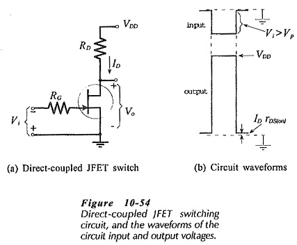
Assuming that VDS(on) is very small, the drain current level is determined from,![]()
Equation 10-21 can be used to determine RD when VDD and ID are specified, or to calculate ID when RD is known. The ID level can then be employed to determine VDS(on). The lowest drain current that can be used must be very much greater than the specified drain-source leakage current for the device.
To switch the FET off, Vi should exceed the maximum pinch-off voltage. However, Vi must not be so large that the drain-gate voltage (VDG = VDD + Vi) approaches the breakdown voltage. A rule-of-thumb is to select the input voltage 1 V larger than VP(max).
![]()
The gate resistor (RG) in the circuit in Fig. 10-54 is provided solely to limit any gate current in the event that the gate-source junctions become forward biased. The circuit might operate satisfactorily with RG selected as 1 MΩ, however, high-value resistors can slow the switching speed of the circuit, so, quite small resistance values are often used for RG.
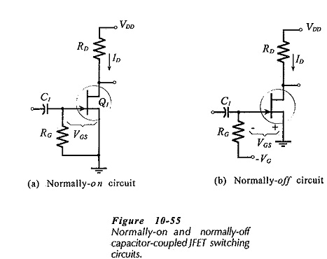
Capacitor-Coupled JFET Switching Circuits:
Two capacitor-coupled Biasing FET Switching Circuits are shown in Fig. 10-55. The FET in Fig. 10-55(a) is normally-on because it has VGS = 0, and the device in Fig. 10-55(b) is normally-off with -VGS greater than the pinch-off voltage. In both circuits, the FET is switched on or off by a capacitor-coupled input pulse. The design procedure for these circuits uses the equations already discussed for the direct coupled Biasing FET Switching Circuits.
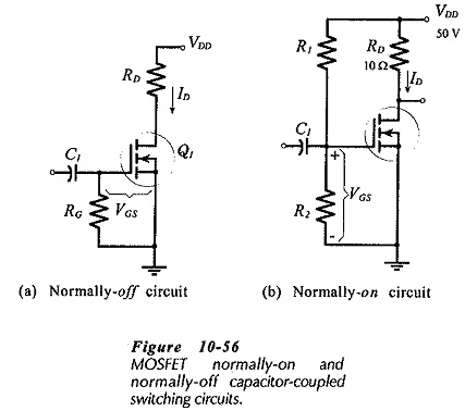
MOSFET Switching:
Figure 10-56 shows two capacitor-coupled MOSFET switching circuits. In Fig. 10-56(a), the FET is biased off because VGS = 0. A positive-going input signal is required to turn the device on. The FET in Fig. 10-56(b) is biased on by the positive VGS provided by R1 and R2. In this case, a negative-going input voltage must be applied to turn the FET off Equations 10-20 and 10-21 can be applied to these circuits to calculate ID and VDS(on). To turn the device on to a desired level of drain current, the transfer characteristics can be employed if they are available.