Output Current Limiting:
Because the output transistors can be destroyed by excessive current flow, output current limiting circuits are often included in a power amplifier. Figure 18-27 shows the typical arrangement for a current limiting circuit.
Emitter resistors RE2 and RE3 are each made up of two components (RA and RB), as illustrated. The Output Current Limiting transistors (Q4 and Q5) are connected as shown, so that the voltage drop across RB2 and RB3 (produced by IL) can turn Q4 and Q5 on. This occurs only when IL is at the selected IL(max) level. When Q4 turns on, it pulls the base of Q2 down, so that Q2 cannot supply current in excess of IL(max). Similarly, turning Q5 on causes the base of Q3 to be pulled up toward its emitter, thus again limiting the output current to IL(max).
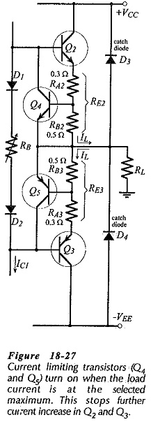
As already discussed for voltage regulator current limiting circuits, Q4 and Q5 typically turn on when VBE ≈ 0.5 V. The component values shown in Fig. 18-27 limit the peak output current to approximately 1 A. Catch diodes D3 and D4 in Fig. 18-27 are usually included with Output Current Limiting, to protect the output transistors from the excessive voltage levels generated in an inductive load when the current growth is limited. The diodes prevent the load voltage from exceeding the supply voltage level.
VBE Multiplier:
Figure 18-28 shows an alternative to diode biasing for the output stage transistors in a Class-AB amplifier. This circuit is known as a VBE multiplier because it produces a bias voltage (VB = VCE6) which is a multiple of the VBE of transistor Q6. Referring to the circuit, note that I10 is the current through the the voltage divider (R10, R11, and R12) that biases Q6. Because I10 is much smaller than IC6, the Q1 collector current (1C1) approximately equals IC6.
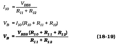
It is seen that the base bias voltage for the output stage transistors can be set by suitable selection of the VBE multiplier resistors. The bias voltage remains constant when IC1 changes. Also, it can also be shown that the changes produced in VB by temperature variations closely match the total VBE temperature changes in the four output stage transistors.