Generalized FET Amplifier Circuit:
The analysis of a common source amplifier with a source resistance RS, a common gate amplifier and a common drain amplifier at low frequencies may be made by considering the Generalized FET Amplifier Circuit given in Fig. 13.55. The Generalized FET Amplifier Circuit consists of three independent signal sources (Vin in series with the gate, Vs in series with the source, and Va in series with the drain).
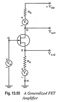
For common source amplifier Va = Vs = 0, and the output Vout1 is taken at the drain terminal D, as shown. For common gate circuit Vin = Va = 0, the input signal is Vs with a source resistance RS, and the output Vout1 is again taken at the drain terminal D. For the common drain (or source follower) RD = 0, Vs = Va = 0, the input signal voltage is Vin and the output Vout2 is taken at the source terminal, as shown in Fig. 13.55. The signal-source resistance is ineffective as it is in series with the gate which draws almost no current.
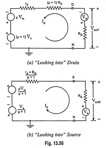
Thevenin’s equivalent circuit from drain to ground and from source to ground are given in Figs. 13.56 (a) and 13.56 (b) respectively. From the circuit given in Fig. 13.56 (a) it is concluded that “looking into the drain” of the FET it is seen (for small signal operation) an equivalent circuit consisting of two generators in series, one of -μ times the gate signal voltage Vin and the second (μ + 1) times the source-signal voltage Vs and the resistance rd+(μ + 1) RS. Note that the source-signal voltage Vs and the resistance in the source lead are both multiplied by the same factor, (μ + 1).
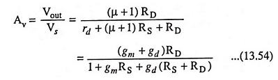
1. Common Source Amplifier With An Unbypassed Source Resistor:
In Fig. 13.56 (a) substituting Va = Vs = 0, we have
Voltage gain
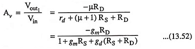
Note that, for RS = 0, the above equation reduces to that Eq. (13.41). The minus sign indicates a phase shift of 180° between input and output.
Resistance Rout, looking into the drain is increased by (μ + 1)RS from its value rd for RS = 0. The net output resistance R′out taking RD into account is given as
![]()
It is observed that with the addition of RS, voltage gain is reduced while the output impedance is increased. The input impedance is extremely high (100 MΩ or so) since gate junction is reverse biased.
2. Common Gate Amplifier:
In Fig. 13.56 (a) substituting Vin = Va = 0, we have
Voltage gain,
Since Av is positive, there is no shift between input and output. Also since gm ≫ gd, the magnitude of amplification is approximately the same as for the common source amplifier circuit with RS ≠ 0.
The output resistance is given by Eq. (13.53), and unless RS is quite small, output resistance will be much larger than rd || RD.
The input impedance Zin, between source and ground is obtained from seeing Fig. 13.56 (b)

The common gate amplifier with its low input impedance and high output impedance has few applications.
Output From Source: From Fig. 13.56 (b) it is concluded that “looking into the source” of the FET it is seen (for small-signal operation) an equivalent circuit consisting of two generators in series, one of value µ/(µ + 1) times the gate-signal voltage vin and the second 1/μ + 1 times the drain-signal voltage va and a resistance rd + RD/μ + 1.
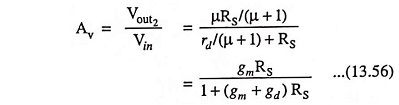
3. Common Drain Amplifier:
Substituting Vs = Va = 0 and RD = 0 in Fig. 13.56 (b), we have
Voltage gain,
The output impedance Zout of the source follower at low frequencies (with RD = 0 and with RS considered external to the amplifier) is, from Fig. 13.56 (b),