What is Single Stage Transistor Amplifier? – Circuit Diagram and its Workings
When only one transistor with associated circuit is used for increasing the strength of a weak signal, the circuit is known as single stage transistor amplifier.
Single Stage Transistor Amplifier Practical Circuit:
A practical circuit of a single stage transistor amplifier in CE configuration and using self-biasing is shown in Fig. 14.2. The resistors R1, R2 and RE form the biasing and stabilization circuit.
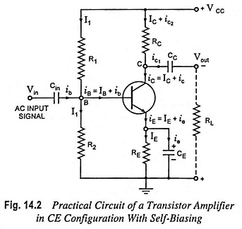
The biasing circuit must establish a proper operating point otherwise a part of the -ve half cycle of the signal may be cut off in the output. The resistor RL connected across the output terminals is called the load. When a number of stages are employed then RL represents the input resistance for the next stage.
An electrolytic capacitor, called the input capacitor, Cin of capacity of about 10 μF is used to couple the signal to the transistor base. In the absence of this capacitor, the signal source resistance will come across R2 and thus change the bias. This capacitor allows only ac signal to flow but isolates the signal source from R2. Another capacitor, called the emitter bypass capacitor CE, of capacity of about 100 μF is used in parallel with emitter resistance RE in order to provide a low reactance path to the amplified ac signal. In the absence of this capacitor, amplified ac signal flowing through RE will cause a voltage drop across it which in turn will feedback the input side and reduce the output voltage.
For coupling of one stage of amplifier to the next stage another capacitor CC, called the coupling or blocking capacitor, of capacity of about 10 μF is used. Because of its presence, the output across the load resistance RL is free from the collector dc voltage. In its absence RC will come in parallel with the resistor R1 of the biasing network of next stage and thereby change the biasing conditions of the next stage.
Various currents flowing in different branches of the amplifier circuit are indicated in Fig. 14.2.
With the application of input signal
![]()
Emitter Bypass Capacitor:
As mentioned above, it is included in the circuit to provide a low reactance path to the amplified ac signal. As shown in Fig. 14.2 it is not connected in series like a coupling capacitor, instead, it is connected across the emitter resistor RE. The reason for doing so is to bypass or shunt ac current away from the emitter resistor RE. When the frequency is high enough it looks like a short. Thus emitter bypass capacitor CE is used to prevent negative feedback in the emitter circuit.
Very simply, negative feedback involves feeding back a portion of the amplifier output signal to its input circuit. Further, the signal is fed back in such a manner that it opposes the input signal. The removal of bypass capacitor results in an increase in the amplifier’s input resistance, a reduction in its voltage gain, and an increase in the output resistance “looking into the collector”. Obviously, an increase in input resistance is a step in the right direction for voltage amplifier. However, a reduction in the voltage gain and increase in the output resistance are generally undesirable effects. Yet there are some advantages offered by these sacrifices. First, even though the voltage gain is reduced, but stability is increased. Specifically, it tends to be less dependent on the transistor’s parameters (e.g., its gm). Second, the increase in the collector-to-ground output resistance makes our approximation of Rout equal to RC even more realistic.
AC Ground:
You may never have heard of an ac ground before, but it really does exist as a separate kind of ground that is different from a mechanical ground. A mechanical ground is achieved by connecting a wire between the point to be grounded and ground.
An ac ground is different because it is produced by connecting a bypass capacitor between the point to be shorted to ground, as far as ac signals are concerned, and the ground, this kind of ground (i.e., ac ground) exists only at high frequencies. In Fig. 14.2 emitter terminal is ac grounded. A designer uses an ac ground when any point needs to be frequency sensitive. Such a point remains normal at low frequencies but grounded at high frequencies.