Universal Transfer Characteristics for FET:
A Universal Transfer Characteristics for FET is simply a transfer characteristic plotted with IDSS = 1 and VP = 1. Then, instead of the scales being calibrated in milliamps and volts, they are marked as the ratios ID/IDSS and VGS/VP. To construct the Universal Transfer Characteristics for FET, Eq. 9-1 is rewritten,
Now, by substituting convenient values for VGS/VP into Eq. 10-18 corresponding values of ID/IDSS are calculated, and these are used to plot the characteristic shown in Fig. 10-45.
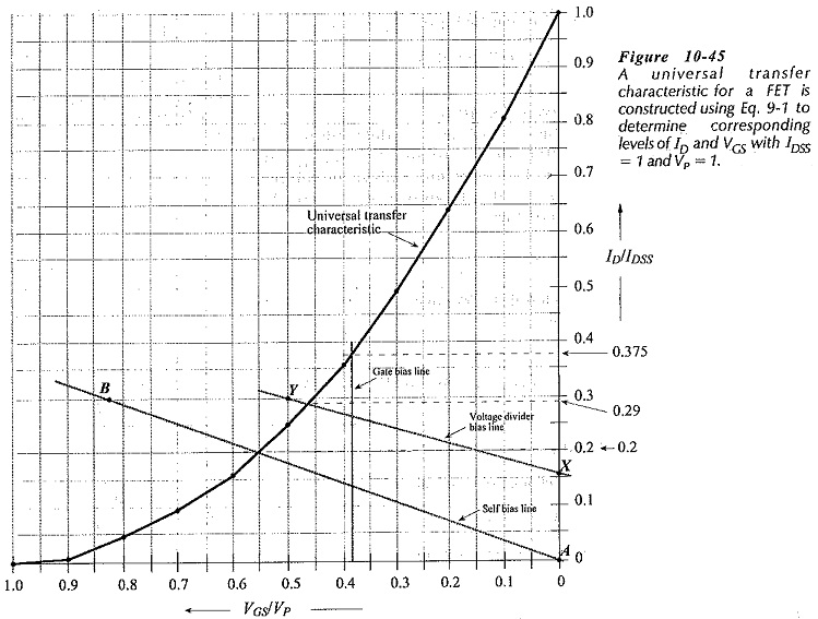
The Universal Transfer Characteristics for FET can be applied to analyze or design a circuit using virtually any JFET. This saves the necessity of plotting the transfer characteristics for each device. The specified values of IDss and Vp must be known for the device. Then, the characteristic is used in the same way as an actual transfer characteristic, except that VGS levels must be converted to VGS/VP ratios, and ID levels must be converted to ID/IDSS before they can be plotted on the graph. Similarly, readings taken from the graph are converted back to VGS and ID levels by multiplying them by Vp and IDss respectively.
Circuit Analysis:
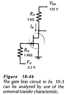
Consider the gate bias circuit analyzed in already, and reproduced in Fig. 10-46. The gate voltage is given as -2.3 V, and the device used has IDSS(max) = 8 mA and VP(max) = -6 V. The bias line is drawn vertically on the Universal Transfer Characteristics for FET at,
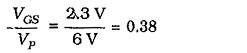
The gate bias line drawn (at VGS/Vp = 0.38) on Fig. 10-45 intersects the universal characteristic at the point where ID/IDSS = 0.375,
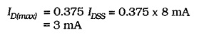
This is the ID(max) level.
The minimum ID for a gate bias circuit can be determined from the Universal Transfer Characteristics for FET, by using the IDSS(min) and VP(min) values. Bias lines can also be drawn for analysis of self bias circuits and voltage divider bias circuits.