Selection of Operating Point in Transistor Biasing:
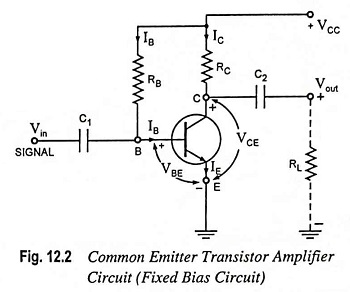
To study the selection of operating point in Transistor biasing conditions on the performance of a transistor, it is necessary to draw a dc load line on the output characteristics of the transistor. Consider the common emitter transistor amplifier circuit shown in Fig. 12.2. The input terminals are base and the emitter and the output is taken from the collector and emitter. Note that the polarity of the transistor terminal voltage in Fig. 12.2 is such that the base-emitter junction is forward biased and collector-base junction is reverse biased. These are the normal bias polarities for the device.
The output characteristics of the transistor are shown in Fig. 12.3. DC load line is drawn on the output characteristics.
In designing a circuit a point on the load line is selected as the dc bias point or quiescent point. This bias point specifies the collector current lC and collector-emitter voltage VCE that exist when no input signal is applied. When an input signal is applied base current varies according to the amplitude of the input signal and causes collector current to vary, consequently producing an output voltage variation.
For faithful amplification of the input signal a judicious selection of the operating or quiescent point is of utmost importance. From our discussion of transistor characteristics, it is clear that the transistor operates linearly when it is constrained to operate in the active region. Once an Operating Point in Transistor Q is established, time-varying excursions of the input signal should cause an output signal (collector current or collector-emitter voltage) of the same waveform. If the output signal is not a faithful reproduction of the input signal, for example, if it is clipped on one side, the operating point is unsatisfactory and needs relocation on the output characteristics. The question now naturally arises as how to choose the Operating Point in Transistor.
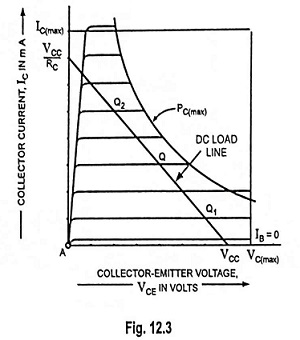
Figure 12.3 provides the output characteristics, with four indicated Operating Point in Transistor used in Fig. 12.2. The biasing circuit may be designed to set the device to operate at any of these points or others within the operating region. The operating region is the area of current or voltage within the maximum limits for the particular device. The maximum ratings, as mentioned in the manufacturer’s specification sheet, are maximum collector current IC(max), maximum collector voltage VC(max), maximum collector dissipation PC(max), and maximum emitter-to-base voltage VBE(max). Figure 12.3 shows three of these bounds on typical output characteristics.
The BJT device could be biased to operate outside these maximum limit points but such an operation would result in either a considerable shortening of lifetime of the device or destruction to the device. Confining ourselves to the safe operating region, we may select several operating points, such as Q, Q1 and Q2. The exact point often depends on the intended use of the circuit. Let us consider some differences between operation at various points shown in Fig. 12.3 to present some basic ideas about the Operating Point in Transistor and, thereby, the bias circuit.
If no bias were used, the device would initially be completely cut off, which would result in zero current through the device and zero voltage across it (i.e., IC = 0 and VCE = 0, as represented by point A). It is, therefore, necessary, to bias the device so that it can respond or cause change in current and voltage for the entire range of an input signal.
Now let us consider point Q, located at the centre of the load line. When a signal is applied to the circuit, in addition to the bias level, collector voltage and current will vary approximately symmetrically around the quiescent values of VC and IC respectively allowing the device to react and amplify both the positive and negative excursions of the input signal. If, as could be the case, the input signal is small, the voltage and current of the device will vary but not enough to drive the device into cutoff or saturation. Cutoff is the condition in which the device no longer conducts. Saturation is the condition in which voltage across the device is the smallest possible with the current in the device reaching a limiting or saturating value depending on the external circuit. The usual amplifier action desired occurs within the operating region of the device, that is, between saturation and cutoff.
At point Q1, near the cutoff region, output current and voltage would be allowed to vary but clipped at the negative peaks for a sinusoidally varying input signal. So this is not a suitable operating point.
At point Q2, near the saturation region, the output signal would be clipped at the positive peaks for a sinusoidally varying input signal. Thus this is also not suitable operating point.
Thus point Q, located at the centre of load line, seems to be the best operating point in terms of linear gain or largest possible voltage and current swing.