Emitter Modulation – Circuit Diagram and its Operation:
The circuit for emitter modulation is shown in Fig. 22.29. It is essentially a CE amplifier. The carrier signal from a crystal oscillator is coupled to the base of amplifier through capacitor Cin. The modulating signal is applied to the emitter circuit. The capacitors Cin and CC are so chosen so as to bypass carrier frequency only.
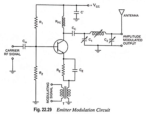
The transformer is employed to provide better matching of the impedance. The voltage divider R1 – R2 and emitter resistance RE provide the proper biasing. The tuned circuit at the collector of the modulator stage eliminates the undesirable signals. The capacitor C’ keeps the RF out of power supply VCC.
The modulating signal, being a part of the biasing circuit, produces low frequency variations in the emitter circuit. The result is that the amplitude of the carrier varies in accordance with the strength of the modulating signal. The amplitude modulated output is obtained at the collector terminal of the amplifier, as shown in Fig. 22.29.
The characteristics of emitter modulation lies in between those of base modulation and collector modulation.