Step Response of an Amplifier:
An alternative criterion of amplifier fidelity is the response of the amplifier to a particular input waveform. Of all possible available waveforms, the most generally useful is the step voltage. In terms of a circuit’s Step Response of an Amplifier, the response to an arbitrary waveform may be written in the form of superposition integral. Another feature that recommends the step voltage is the fact that this waveform is one which permits small distortions to stand out clearly. Additionally, from an experiment point of view, it may be noted that excellent pulse (a short step) and square-wave (a repeated step) generators are available commercially.
As long as an amplifier can be represented by a dominant pole, the correlation between its frequency response and the output waveform for a step input is that given below. Quite often, even for more complicated amplifier circuits, there is an intimate relationship between the distortion of the leading edge of a step and the high-frequency response. Similarly, there is a close relationship between the low-frequency response and the distortion of the flat portion of the step. Such a relationship is expected, because the high-frequency response measures essentially the ability of the amplifier to respond faithfully to rapid variation in signal, while the low-frequency response measures the fidelity of the amplifier for slowly varying signals. An important feature of a step is that it is a combination of the most abrupt voltage change possible and of the slowest possible variation in voltage.
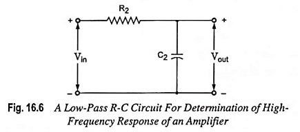
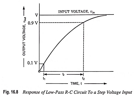
Rise Time: The response of low-pass circuit shown in Fig. 16.6 to a step input of amplitude V is exponential with a time constant τ = R2C2. Since the output voltage (voltage across the capacitor) cannot change instantaneously, the output starts from zero and rises toward the steady-state value exponentially as depicted in Fig. 16.8. The output voltage is given by the equation
![]()
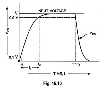
The time required for output voltage vout to attain one-tenth of its final value is 0.1R2C2, and the time to attain nine-tenths its final value is 2.3R2C2. The difference between the two, known as rise time tr of the circuit is 2.2R2C2. The time tr indicates how fast the amplifier can respond to a discontinuity in the input voltage.
Substituting R2C2 = 1/2πf2 from Eq. (16.31) in equation for tr, we have
Rise time,
![]()
i.e. rise time is inversely proportional to the upper 3-dB frequency. For an amplifier having bandwidth of 1 MHz bandpass, tr = 0.35 μs.
Pulse Input: The response to a pulse, for times less than the pulse width tp is the same as that for a step input because pulse signal is same as step input for t < tp. However, at the end of the pulse, as the input becomes zero, the output also drops exponentially to zero. The reason is that capacitor voltage falls exponentially to zero, as the input becomes zero.
Thus output for pulse input is given as
![]()
At t = tp,
![]()
At t = tp, input voltage becomes zero but since the voltage across a capacitor cannot change instantaneously, output remains the same as it is at t = tp. After that capacitor starts getting discharged through resistance R2 and voltage across it drops exponentially to zero. Hence output voltage for t > tp.
![]()
The above equation is discharging equation of capacitor delayed by time tp. Hence output voltage must be decreasing towards zero for t > tp. This is illustrated in Fig. 16.9.
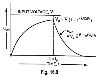
It shows that output voltage will always extend beyond pulse width tp. This is because the charge stored on capacitor during pulse cannot leak off instantaneously.
It is also observed from Fig. 16.9 that output shape is different from that of input i.e. there is distortion. Distortion may be reduced by making rise time much smaller than pulse width tp. For a circuit having f2 equal to 1/tp, tr = 0.35 tp. For this value of tr output will be of the shape shown in Fig. 16.10, which is not exact but approximately reproduction of the input.
As a thumb rule it can be said:
A pulse shape will be preserved if the 3-dB frequency is approximately equal to the reciprocal of the pulse width (PW).
Thus to pass a 0.2 μs pulse reasonably well needs a circuit with an upper cutoff frequency of the order of 5 MHz.
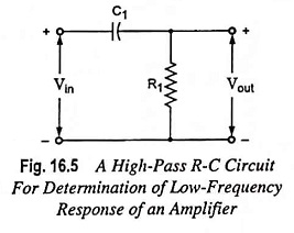
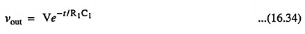
Tilt or Sag: If a step of amplitude V is impressed on the high-pass circuit shown in Fig. 16.5, the output is given by
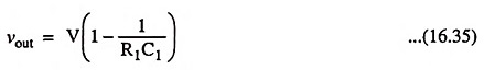
For times t << R1C1, the response is given by
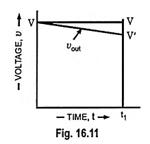
From Fig. 16.11, it is seen that the output is tilted, and the percent tilt, or sag in time t1 is given by
It is found that the same expression is valid for the tilt of each half cycle of a symmetrical square wave of peak-to-peak value V and period T provided that t1 = T/2. If f = 1/T is the frequency of a square wave, then tilt may be expressed in the form
Thus, tilt is directly proportional to the lower 3-dB frequency. For passing a 50 Hz square wave with less than 10 per cent sag, lower 3-dB frequency, f1 must not exceed 1.6 Hz.