Step Down Converter:
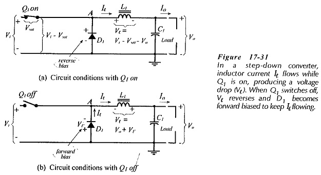
A step-down switching regulator, or Step Down Converter (also termed a buck converter), produces a dc output voltage lower than its input voltage. The basic circuit arrangement for a step-down converter is shown in Fig. 17-30. Note the presence of the catch diode (D1). This is normally reverse biased when Q1 is on, but becomes forward biased when Q1 switches off.
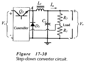
Figure 17-31(a) illustrates the situation when Q1 is on (in saturation). Inductor current (Il) flows from Vi, producing an inductor voltage drop (Vl) which is + on the left, – on the right. At this time D1 is reverse biased. When Q1 switches off [Fig. 17-31(b)], the inductor has stored energy, and it opposes any change in current level. In order to maintain inductor current flow (with Q1 off), the inductor voltage reverses, becoming – on the left, + on the right, as illustrated. The reversed polarity of Vl forward biases D1 to provide a path for Il. If D1 was not present in the circuit, the inductor voltage would become large enough to break down the Junctions of Q1. So, D1 catches Vl and stops it from increasing; hence the name catch diode.
Step-Down Converter Equations:
Figure 17-32 shows the circuit waveforms during the Q1 on and off times (ton and toff). These are; switch voltage (VA) at point A (Q1 emitter), inductor voltage (Vl), inductor current (Il), and output voltage (Vo). Equations for calculating component values can be derived by considering the circuit conditions and the waveforms.
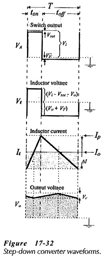
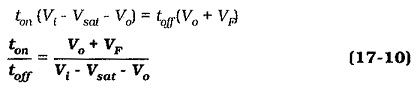
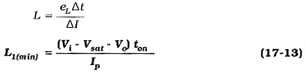
The input voltage (Vl) appears at the collector of transistor Q1. When Q1 is on, the voltage across the inductor and capacitor (in series) is (Vi – Vsat), and the inductor voltage is (Vi – Vsat – Vo), [see Fig. 17-31(a)]. When Q1 switches off, the inductor voltage becomes (Vo + VF), [Fig. 17-31(b)]. Typically, VF = 0.7 V, and Vsat ranges from 0.2 V to 1.5 V, depending on the transistor and the load current. The energy supplied to the inductor during ton is proportional to [ton X (Vi – Vsat – Vo)], and the energy supplied by the inductor to the output during toff is proportional to [toff X (Vo + VF)]. Because the inductor input energy must equal its output energy,
From Fig. 17-32,
![]()
The inductor is charged from the supply via Q1 during ton and it discharges to the load and the output capacitor via D1 during toff. When the output current is a maximum (Io(max)), the inductor current (Il) can be allowed to change from zero to a peak level.
![]()
This is the absolute maximum inductor current change (ΔI = IP) that can occur when the circuit is operating correctly.
An equation for the inductance may be derived from a knowledge of the inductor voltage and the inductor current change during ton.
The output voltage waveform (Fig. 17-32) is also the capacitor voltage waveform. As illustrated, the capacitor voltage increases while Il is greater than Io, and decreases during the time that Il is less than Io. While Il is less than Io, the average inductor current is ΔI/4 below Io, and the capacitor must supply this current to the load. The time involved is T/2, and the capacitor voltage change is the peak-to-peak output ripple voltage (Vr). So, an equation for the minimum capacitance of C1 can be derived as,
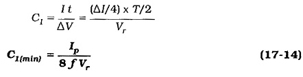
It should be noted that Equations 17-13 and 17-14 give minimum inductor and capacitor values. The use of component values larger than the minimum will result in a lower ripple voltage at the regulator output.
When selecting components, the capacitor equivalent series resistance (ESR) and the inductor winding resistance (RW) must be taken into account. ESR can affect the output ripple voltage. The maximum ESR should usually be limited to (0.1 Vr/ΔI). If RW is too large, it will produce an excessive voltage drop across the inductor. The maximum winding resistive voltage drop should typically not exceed 0.2 V. Also, the peak level of the inductor current must be passed without saturating the core.
Resistance values for R1 and R2 (in Fig. 17-30) depend on the output and reference voltages.