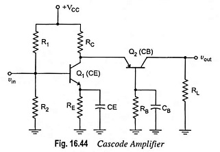
Cascode Amplifier or CE-CB Configuration:
The CE-CB configuration (usually referred to as cascode amplifier) is shown in Fig. 16.44. Figure 16.44 shows a cascode configuration with a common-emitter (CE) stage feeding a common-base (CB) stage. This configuration of course, has basically the input characteristics similar to those of CE amplifier and output characteristics similar to those of CB amplifier. More specifically, it has high output resistance and is inherently more stable. The high output resistance is useful in achieving large voltage gain. This arrangement is designed to provide a high input impedance with low voltage gain to ensure that the input Miller capacitance is at a minimum with the CB stage providing good high-frequency operation.
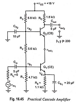
A practical version of a cascode amplifier is given in Fig. 16.45.
DC Analysis:
In a cascode amplifier depicted in Fig. 16.45 R1, R2 and R3 form a bias network for transistors Q1 and Q2; CS1 and CS2 provide ac signal ground paths from the Q1 emitter and Q2 base, respectively; Cin is the coupling capacitor. For the proper operation of the circuit it is necessary that transistors Q1 and Q2 must be identical.
For dc conditions all capacitors are assumed to be open circuited.
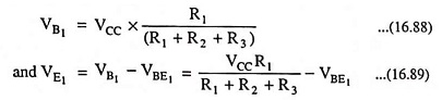
Applying voltage divider rule, we have
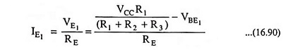
Emitter current of transistor Q1,
Once the emitter current of transistor Q1 is known, all other currents in and voltages at the three terminals for Q1 and Q2 can be readily determined if required.
AC Analysis:
Figure 16.46 depicts the small-signal T-equivalent circuit for the cascode amplifier given in Fig. 16.45. Here we will determine low-frequency, small-signal properties (like voltage gain, current gain and input resistance) of the cascode amplifier circuit. In low-frequency analysis, all capacitors are considered short elements.
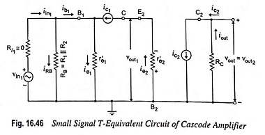
In Fig. 16.46, RB = R1 || R2; r′e1 ≡ r′e2 because IE1 ≡ IE2; and Vout1 is the output voltage of the CE stage. Since Q1 and Q2 are identical transistors, βac1 = βac2 and βdc1 = βdc2 and subscripts will be omitted in the calculations that follow.
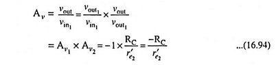
1. Voltage Gain: For the input circuit given in Fig. 16.46, since RB ≫ r′e1, vin1 = r′e1ie1 and vout1 = – r′e2ie2
Since, ie2 = ic1 and ic1 ≡ ie1, it means that ie1 ≡ ie2.
Voltage gain of CE stage is
The output voltage,
Substituting the value of ie2 from above equation in Eq. (16.92), we have
![]()
Then the voltage gain of CB stage is
Thus overall voltage gain of the cascode (CE-CB) configuration
2. Current Gain: The current gain Ai of the cascode (CE-CB) configuration may be expressed as
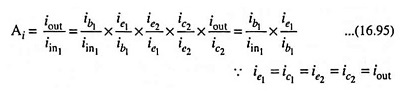
Applying the current divider rule to the input circuit, we have
Thus, the current gain Eq. (16.95) becomes

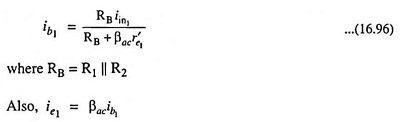
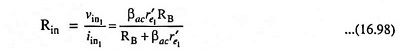
3. Input Resistance: For input circuit,
![]()
Substituting the value of ib1 from Eq. (16.96) in above equation, we have
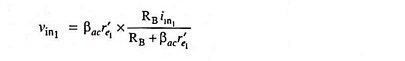
and Input resistance,
The cascode amplifier shown in Fig. 16.44 is not encountered very often in discrete circuitry because (i) it needs a large number of resistors and capacitors for providing bias and preventing unwanted feedback and (ii) it does not offer much flexibility as the IC cascode amplifier does.