Minimum Mode Configuration of 8086:
Pin definitions from 24 to 31 are different for minimum mode and maximum mode. By using these pins the 8086 itself generates all bus control signals in the Minimum Mode Configuration of 8086. These signals are :
Pin Definitions (24 to 31) in Minimum Mode:
INTA (Interrupt Acknowledge) Output : This indicates recognition of an interrupt request. It consists of two negative going pulses in two consecutive bus cycles. The first pulse informs the interface that its request has been recognized and upon receipt of the second pulse, the interface is to send the interrupt type to the processor over the data bus.
ALE (Address Latch Enable) output : This signal is provided by 8086 to demultiplex the AD0-AD15 into A0-A15 and D0-D15 using external latches.
DEN (Data Enable) output : This signal informs the transceivers that the CPU is ready to send or receive data.
DT/R (Data transmit/Receive) output : This signal is used to control data flow direction. High on this pin indicates that the 8086 is transmitting the data and low indicates that the 8086 is receiving the data.
M/IO output : It is used to distinguish memory data transfer, (M/I0 = HIGH) and I/O data transfer (M/I0 = LOW).
WR : Write output : WR is low whenever the 8086 is writing data into memory or an I/O device.
HOLD input, HLDA output : A HIGH on HOLD pin indicates that another master (DMA) is requesting to take over the system bus. On receiving HOLD signal processor outputs HLDA signal HIGH as an acknowledgment. At the same time, processor tristates the system bus. A low on HOLD gives the system bus control back to the processor. Processor then outputs low signal on HLDA.
Minimum Mode Configuration:
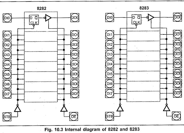
Fig. 10.2 shows the typical Minimum Mode Configuration of 8086. As shown in the figure, AD0-AD15, A16/S3-A19/S6, and BHE/S7 signals are multiplexed. These signals are demultiplexed by external latches and ALE signal– generated by the processor. This is accomplished by using three latch ICs (Intel 8282/8283), two of them are required for a 16-bit address and three are needed if a full 20-bit address is used. Fig. 10.3 shows the internal block diagram of 8282/8283 latches. The 8282 provides noninverting outputs while the 8283 version inverts the input data. In addition to their demultiplexing function, these chips also buffer the address lines, providing increased output driving capability. The output low level is specified as 0.45 V maximum with a sink current of 32 mA maximum. The high level is specified as 2.4 V minimum while supplying a 5 mA maximum high level load current.
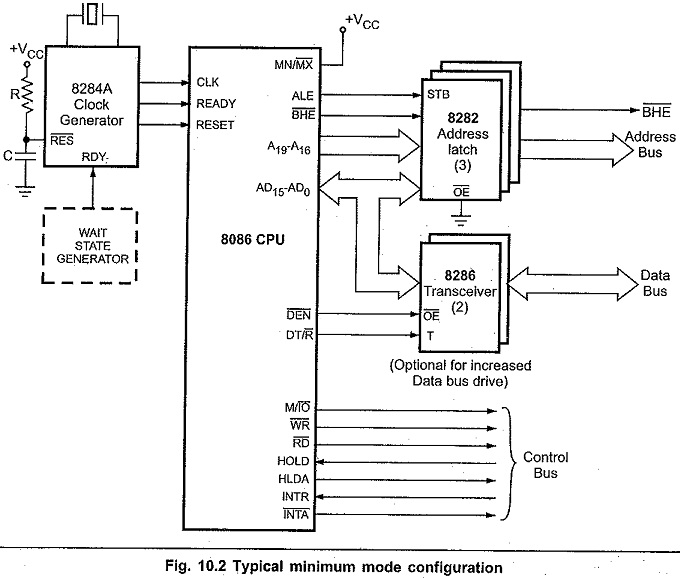
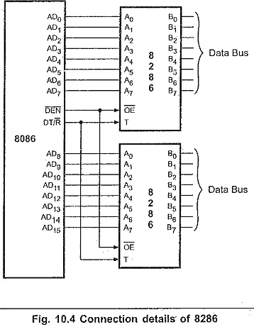
If a system includes several interfaces then to increase current sourcing/sinking capacities it is necessary to use drivers and receivers (transceiver) for data bus also. The Intel 8286 device is used to implement the transceiver block shown in Fig. 10.2. The 8286 contains 16 tristate elements, eight receivers, and eight drivers. Therefore two 8286s are required to service 16 data lines of 8086. Fig. 10.4 shows the detailed connections of 8286.
DT/R signal is connected to the T input, which controls the direction of the data flow. When this signal is low, receivers are enabled, so that 8086 can read data from memory or input device. To write data into memory or output device, the 8086’s DT/R signal goes high. Due to this drivers are enabled to transfer data from 8086 to the memory or the output device. At the time of data transfer, to enable output of transceiver its OE should be low. This is accomplished by connecting DEN signal of 8086 to the OE pin of 8286, since DEN signal goes low when CPU is ready to send or receive data.
The third component. other than the processor that appears in Fig. 10.2 is an 8284 clock generator. The 8284 clock generator does the following functions
- Clock generation
- RESET synchronization
- READY synchronization
- Peripheral clock generation.
The Fig. 10.5 shows the internal logic diagram of 8284.
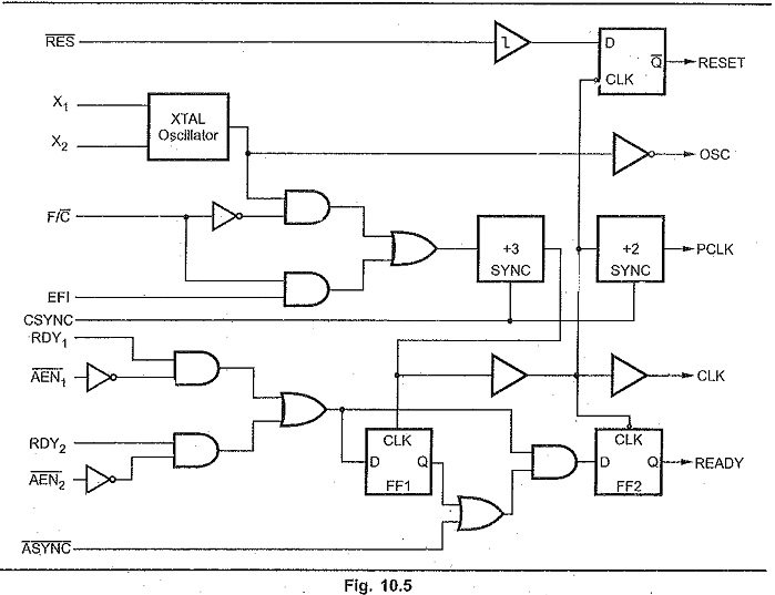
The top half of the logic diagram represents the clock and reset synchronization section of the 8284 clock generator. As shown in the logic diagram, the crystal oscillator has two inputs : X1 and X2. If a crystal is attached to X1 and X2, the oscillator generates a square-wave signal at the same frequency as the crystal. The output of oscillator is fed to an AND gate and also to an inverter buffer that provides the osc output signal. The F/C signal selects one of the oscillator inputs. When F/C input is 1, the EFI input determines the frequency; otherwise oscillator determines the frequency. When EFI input is used, CSYNC signal is used for multiple buffered before it leaves the clock generator. As shown in the Fig. 10.5, the output of the divide-by-3 counter generates the timing for ready synchronization, a signal for another counter (divide-by-2), and the CLK signal to the 8086/8088 microprocessors. The two cascaded counters (divide-by-3 and divide-by-2) provide the divide-by-6 output at PCLK, which can be used to provide clock input for peripherals. The address enable pins, AEN1 and AEN2 are provided to qualify the bus ready signals, RDY1 and RDY2, respectively.
The reset circuit of 8284 consists of a schmitt trigger buffer and a single D flip-flop circuit. The D flip-flop ensures that the timing requirements of the 8086/8088 RESET input are met. This circuit applies the RESET signal to the microprocessor on the negative edge. (1 to 0 transition) of each clock. The 8086/8088 microprocessors sample RESET at the positive edge (0 to 1 transition) of the clocks; therefore, this circuit meets the timing requirements of the 8086/8088.
The Fig. 10.6 shows the circuit connection for 8284 clock generator. The RC circuit provides a logic 0 to the RES input pin when power is first applied to the system. After a short time, the RES input becomes a logic 1 because the capacitor charges toward + 5.0 V through the register. A push button switch allows the microprocessor to be reset by the operator.

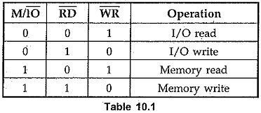
The status on the M/IO, RD, and WR lines decides the type of data transfer, as listed in the Table 10.1.
HOLD and HLDA signals are used to interface other bus masters like DMA controller. Interrupt request (INTR) and interrupt acknowledge (INTA) are used to extend the interrupt handling capacity of the 8086 with the help of interrupt controller.
Bus Timings for Minimum Mode:
The timing diagrams of input and output transfers for Minimum Mode Configuration of 8086 are shown in the Fig. 10.7 (a) and (b) respectively. These are explained in steps.
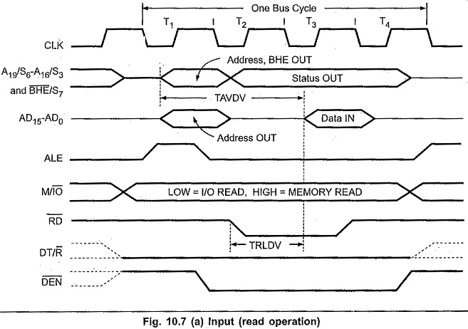
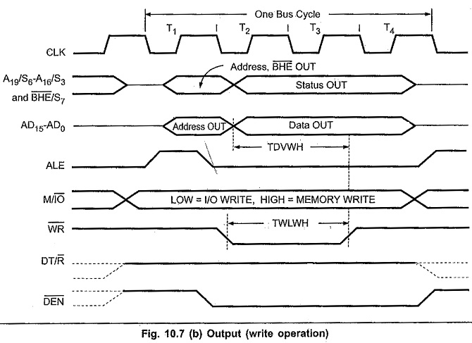
- When processor is ready to initiate the bus cycle, it applies a pulse to ALE during T1. Before the falling edge of ALE, the address, BHE, M/IO, DEN and DT/R must be stable i.e. DEN = high and DT/R = 0 for input or DT/R = 1 for output.
- At the trailing edge of ALE, ICs 74LS373 or 8282 latches the address.
- During T2 the address signals are disabled and S3-S7 are available on AD16/S3-AD19/S6 and BHE/S7. Also DEN is lowered to enable transceiver.
- In case of input operation, RD is activated during T2 and AD0 to AD15 go in high impedance preparing for input.
- If memory or I/O interface can perform the transfer immeaiately; there are no wait states and data is output on the bus during T3.
- After the data is accepted by the processor, RD is raised high at the beginning of T4.
- Upon detecting this transition during T4, the memory or I/O device will disable its data signals.
- For an output operation, processor applies WR = 0 and then the data on the data bus during T2.
- In T4, WR is raised high and data signals are disabled.
- For either input or output operation, DEN is raised during T4 to disable the Also M/IO is set according to the next transfer at this time or during next T1 state. Thus length of bus cycle in 8086 is four clock cycle. If the bus is to be inactive after completion of bus cycle, then the gap between the successive cycles is filled by ideal state clock cycles.
When the memory or I/O device is not able to respond quickly during transfer, wait states (Tw) are inserted between T3 and T4 by disabling the READY input of the 8086. The bus activity during wait state is same as during T3.