Maximum Mode Configuration of 8086:
A processor is in the Maximum Mode Configuration of 8086 when its MN/MX pin is grounded. The maximum mode defines pins 24 to 31 as follows:
Pin Definitions (24 to 31) in Maximum Mode:
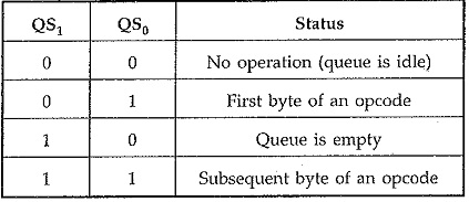
1.QS1, QS0 (output) : These two output signals reflect the status of the instruction queue. This status indicates the activity in the queue during the previous clock cycle.
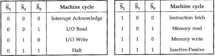
2.S2,S1,S0 (output) : These three status signals indicate the type of transfer to be take place during the current bus cycle.
3.LOCK : This signal indicates that an instruction with a LOCK prefix is being executed and the bus is not to be used by another processor:
4.RQ/GT1 and RQ/GT0 : In the Maximum Mode Configuration of 8086, HOLD and HLDA pins are replaced by RQ (Bus request)/GT0 (Bus Grant), and RQ/GT1 signals. By using bus request signal another master, can request for the system bus and processor communicate.that the request is granted to the requesting master by using bus grantnal. Both signals are similar except the RQ/GT0 has higher priority than RQ/GT1.
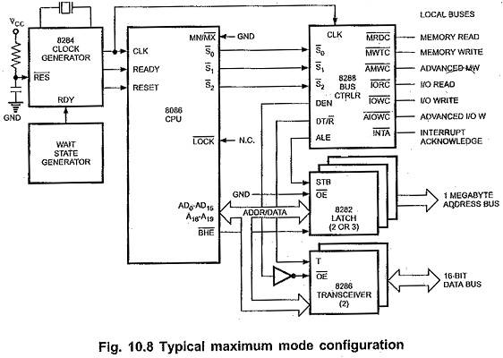
Fig. 10.8 shows the typical Maximum Mode Configuration of 8086. In the maximum mode additional circuitry is required to translate the control signals. The additional circuitry converts the status signals (S2-S0) into the I/O and memory transfer signals. It also generates the control signals required to direct the data flow and for controlling 8282 latches and 8286 transceivers. The Intel 8288 bus controller is used to implement this control circuitry.
8288 Bus Controller Block Diagram:
Fig. 10.9 shows that the 8288 bus controller is able to originate the address latch enable signal to the 8282’s, the enable and direction signals to the 8286 transceivers, and the interrupt acknowledge signal to the interrupt controller. It also decodes the S2-S0 signals to generate MRDC, MWTC, IORC, IOWC, MCE/PDEN, AEN, IOB, CEN, AIOWC, and AMWC signals.
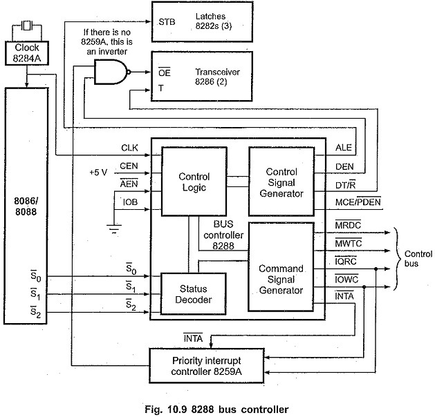
MRDC (Memory Read Command) : It instructs the memory to put the contents of the addressed location on the data bus.
MWTC (Memory Write Command) : It instructs the memory to accept the data on the data bus and load the data into the addressed memory location.
IORC (I/O Read Command) : It instructs an I/O device to put the data contained in the addressed port on the data bus.
IOWC (I/0 Write Command) : It instructs an I/O device to accept the data on the data bus and load the data into the addressed port.
MCE/PDEN (Master Cascade Enable/Peripheral Data Enable) : It controls the mode of operation of 8259. It selects cascade operation for 8259 (interrupt controller) if IOB signal is grounded and enables the I/O bus transceivers if IOB is tied high.
AEN, IOB and CEN : These pins are used in multiprocessor system. With a single processor in the system, AEN and IOB are grounded and CEN is tied high. AEN causes the 8288 to enable the memory control signals. IOB (I/O bus mode) signal selects either the I/O bus mode or system bus mode operation. CEN (control enable) input enables the command output pins on the 8288.
AIOWC/AMWC (Advance I/O Write Command/Advance Memory Write Command) : These signals are similar to IOWC and MWTC except that they are activated one clock pulse earlier. This gives slow interfaces an extra clock cycle to prepare to input the data.
Bus Timing Diagram of 8086:
The Bus Timing Diagram of 8086 of input and output transfers are shown in the Fig. 10.10 (a) and (b) respectively.
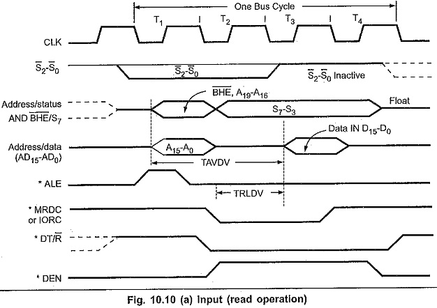
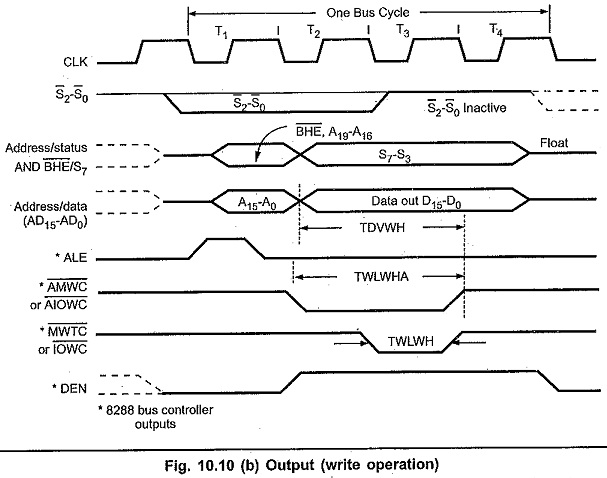
These are explained in steps.
- S0,S1,S2 are set at the beginning of bus cycle. On detecting the change on
passive state S0 = S1 = S2 = 1, the 8288 bus controller will output a pulse on its ALE and apply a required signal to its DT/R pin during T1. - In T2, 8288 will set DEN = 1 thus enabling transceiver. For an input, 8288 it will activates MRDC or IORC. These signals are activated until T4. For an output, the AMWC or AIOWC is activated from T2 to T4 and MWTC or IOWC is activated from T3 to T4.
- The status bits S0 to S2 remain active until T3, and become passive during T3 and T4.
- If ready input is not activated before T3, wait state will be inserted between T3 and T4.