High Pass RC Circuit Diagram, Derivation and Application:
The High Pass RC Circuit is shown in Fig. 29.1. The reactance of the capacitor is given as
![]()
i.e., Reactance XC of the circuit capacitor decreases with the increase in frequency. Thus at low frequencies the capacitor C offers considerable reactance and so blocks them, but at higher frequencies it offers little reactance and allows them to pass through it. The output voltage is developed across resistor R.
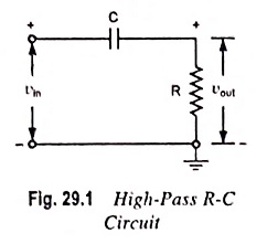
With the increase in frequency, the reactance of the capacitor decreases and, therefore, the output and gain increase. At very high frequencies, the capacitive reactance becomes very small, so the output becomes almost equal to the input and gain becomes equal to unity. Since this circuit attenuates the low-frequency signals and allows transmission of high-frequency signals with little or no attenuation, it is called a High Pass RC Circuit.
Because of its blocking property for dc or low frequency input signals the capacitor acts like an open circuit and blocks the signal. This is the reason that the capacitor in the circuit is called the blocking capacitor. This circuit is widely employed as a coupling circuit to provide isolation between input and output.
Now response of the High Pass RC Circuit for different types of inputs will be found.
Response of High Pass RC Circuit to Standard Waveforms:
1. Sinusoidal Input:
For a sinusoidal input the waveshape of the output will remain the same; the output will differ only in amplitude and phase angle depending on the frequency of the input signal. Here we are concerned only with amplification of the signal which is expressed as

The current through the circuit is given as

and output voltage,

So gain,
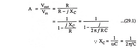
From above equation it is obvious that for a given circuit, the gain A depends upon the frequency of the input signal.
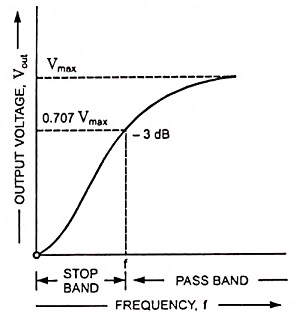
The frequency response curve for the circuit is given in Fig. 29.2. From frequency response curve it is obvious that all frequencies above cutoff frequency f, are passed while those below are attenuated. At cutoff frequency R = XC, the phase angle is 45° and output power is half of the input power. The output voltage is 0.707 times the maximum value of voltage Vmax. The cutoff frequency is given as

Substituting 1/2πRC = f1 in Eq, (29.1) we have

Now magnitude of A and phase angle θ are given as

and phase angle
![]()
As
![]()
When

f1 is also known as low 3-dB frequency.
f = f1 also implies that
![]()
So f1 is the frequency at which capacitive reactance is equal to the resistance of the circuit.
The maximum possible value of gain (unity) is approached asymptotically at high frequencies.
The lower cutoff frequency of a High Pass RC Circuit, f1 produces a tilt.
For a 10 per cent change in capacitor voltage, the time or pulse width involved is
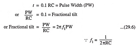
The above equation applies when the tilt is 10 per cent or less. When the tilt exceeds 10%, the output voltage should be treated as exponential instead of linear and is given by an expression
![]()
where τ = RC, is called the time constant of the circuit.
2. Step Input:
As already discussed in Art. 28.6, a step voltage is zero for all times when t < 0 and maintains a voltage level, say V, for all times when t ≥ 0. The transition from voltage level 0 to V occurs at t = 0 and is instantaneous. Instant of time just before the transition occurs is denoted by t = 0– and instant of time just after the transition has taken place is denoted by t = 0+.
At instant t = 0–, since the input is zero, the output is also zero. At instant t = 0, the input suddenly becomes V. Since the voltage across a capacitor cannot change instantaneously, the output voltage remains V. At t = 0+ the input voltage remains unchanged at V, the capacitor starts charging exponentially with time constant RC. As the capacitor C charges exponentially to V, the output voltage Vout falls exponentially to zero. When the capacitor gets charged to V volts, the output voltage will be obviously zero, as illustrated in Fig. 29.3.
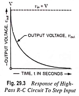
The rate at which the output voltage drops to zero exponentially depends upon the time constant RC of the circuit.
Input voltage,

From the circuit shown in Fig. 29.1.
Output voltage,
![]()
Since at any instant input voltage,
Taking Laplace of this

Assuming zero charge on capacitor at time instant t = 0
Taking inverse Laplace we have
![]()
where τ = Time constant of the circuit = RC
Note that the output voltage is equal to input voltage or initial value at t = 0; 0.607 times of initial value at t = 0.5 T; 0.368 times of initial value at t = T; 0.135 times of initial value at t = 2T and 0 at t = ∞. The output has completed more than 95 per cent of its total change after 3T and more than 99 per cent of its swing when t > 5T. Hence, although the steady-state is approached asymptotically, we may assume for most applications that the final value has been reached after 5T.
The voltage across a capacitor can change instantaneously only when an infinite current passes through it.
3. Pulse Input:
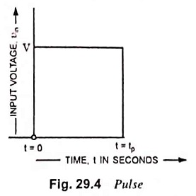
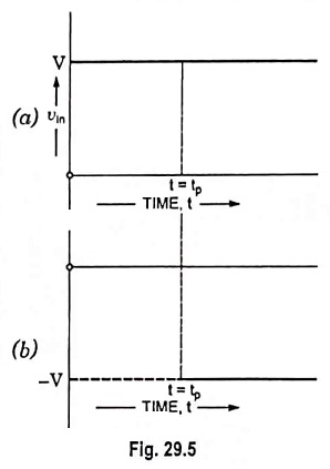
An ideal pulse voltage waveform is given in Fig. 29.4. Here V is amplitude of pulse and tp is pulse duration or pulse width.
Input voltage,

As discussed in Art. 24.8, a pulse can be considered as a sum of two step voltages (i.e., a step of amplitude +V starting at t = 0 and a step voltage of -V appearing at t = tp, as illustrated in Fig. 29.5 (a) and 29.5 (b) respectively. The sum of these two steps is the pulse shown in Fig. 29.4.
For t < 0, the input is zero and the output is also zero. At t = 0, there is a positive step of V at the input. Since voltage across the capacitor cannot change instantaneously, the changes in input appear at the output in totality. Hence the output at t = 0 is V. For time t, 0 ≤ t ≤ tp input is constant at V, the capacitor charges to V and the output falls exponentially to zero.
![]()
The above expression was derived in the previous subsection

At the input at, t=tp, there is a negative step of V and again this step will appear at the output

Since V > Ve-tp/CR at t = tp, vout is negative, as illustrated in
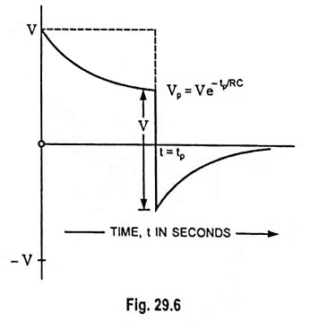
Fig. 29.6. Now, input is zero, the capacitor discharges to zero exponentially and the output voltage rises to 0 exponentially. For t > tp, output voltage is given as
![]()
The rate of exponential fall or rise depends upon the time constant RC. The response for RC >> tp and for RC << tp is shown in Fig. 29.7 (a) and (b). If the time constant is very small, we get positive and negative spikes. The process of converting pulses into spikes is known as peaking.
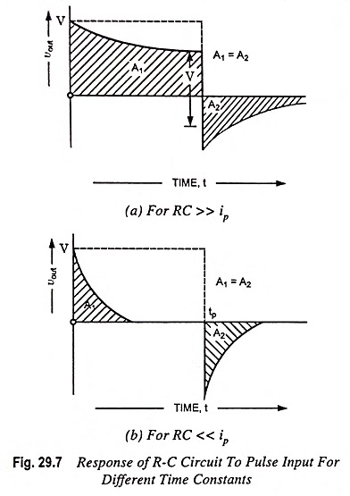
The areas A1 and A2 above and below the zero axis are equal which means dc component of output voltage is always zero.
In any case, for any value of RC, there must always be a tilt and an undershoot. The undershoot can be minimised by making RC very large in comparison to pulse width tp. However, the area below the zero axis will always be equal to the area above the axis A1 = A2. That is why output below zero axis rises to zero very slowly for RC >> tp.
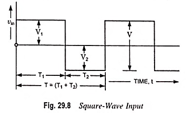
4. Square-Wave Input:
If a number of pulses of alternative positive and negative amplitude occur respectively, a square wave is formed. Also a square wave consists of a number of positive and negative unit step functions having their discontinuity at certain intervals of time.
A square wave may alternatively be defined as a waveform which maintains itself at one constant level V1 for a time duration of T1 and another constant level V2 for time duration of T2 and which repeats itself at time T = T1 + T2.
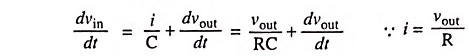
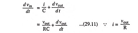
For any periodic input waveform, the output is also a periodic waveform of same period and the average level of the steady state output signal is always zero and is independent of the dc level of the input. This is due to blocking property of the capacitor. This can be shown as below.
Since at any instant, input voltage vin is equal to potential difference across resistor plus potential difference across the capacitor,

Differentiating above equation w.r.t. time we have
Multiplying by dt and then integrating over time period T, we have
Under steady-state conditions, the output waveform is repetitive with a period T so that
The above integral represents the area under the output waveform over one cycle. It implies that the average level of a steady-state output signal is always zero. It shows that output must extend in both the positive and negative directions of zero axis, so that the area above the axis must be equal to the area below the axis making resultant area equal to zero.
For square wave, output is same as for pulse input only the output in this case is repetitive with alternate positive and negative amplitude.
The shape of the output waveform in this case is going to depend upon the time constant RC. If RC/T1 and RC/T2 are both arbitrarily large in comparison with unity, the output will be identical to the input waveform. On the other hand, if RC/T1 and RC/T2 are both very small as compared to unity, the output will consist of alternate positive and negative peaks with having peak-to-peak amplitude twice that of the input, as illustrated in Fig. 29.9 (b).
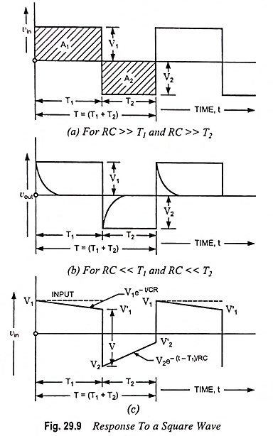
Analysis: For a constant voltage applied to the circuit shown in Fig. 29.1, output at any instant is given as
![]()
When a square-wave signal shown in Fig. 29.8 is applied to the circuit shown in Fig. 29.1. the output is as follows.
From Fig. 29.9 (c)
At time t = 0,
![]()
At time t = T1,

At time t = T1 + T2,

For a symmetrical square-wave

Substituting these values in above equations we have

Eliminating V′1 we have
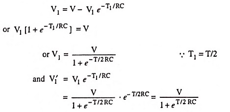
For T/2RC << 1 these reduce to
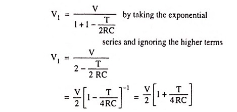
by taking binomial and ignoring the higher terms.
Similarly

The percentage tilt P is defined as
![]()
Since the lower cutoff frequency – 3-dB point is given by f1 = 1/2πRC.

where f = 1/T is the frequency of the square-wave applied to the R-C circuit.
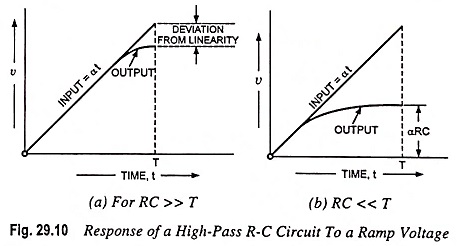
5. Ramp Input:
A waveform which is zero for t < 0 and which increases linearly with time for t > 0, ν = α t, is known as a ramp or sweep voltage. Such a waveform is shown in Fig. 29.10 (a). When the High Pass RC Circuit shown in Fig. 29.1 is excited by a ramp input vin(t) = αt where α is the slope of the ramp.
Since at any instant input voltage vin is equal to pd across resistor plus pd across the capacitor,

Differentiating above equation w.r.t. time we have
The above equation has the solution, for vout = 0 at t = 0,
![]()
For times t which are very small in comparison with RC, we have
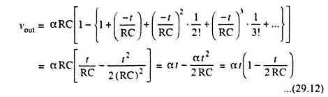
Figure 29.10 depicts the response of the High Pass RC Circuit for a ramp input when (a) RC >> T and (b) RC << T where T is the ramp duration. The output signal falls away slightly from the input, as depicted in Fig. 29.10 (a). As a measure of the departure from linearity, let us define the transmission error et as the difference between input and output divided by the input. The error at time t = T is then
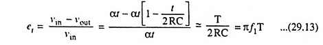
where f1 = 1/2πRC is again the lower 3-dB frequency of the High Pass RC Circuit.
For large values of t in comparison with RC, the output approaches the constant value α RC as depicted in Fig. 29.10 (b).
6. Exponential Input:
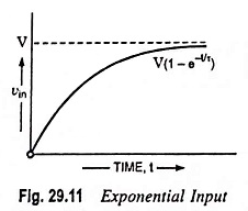
When an exponential input
![]()
shown in Fig. 29.11 is applied to a High Pass RC Circuit shown in Fig. 29.1, Eq. (29.11) becomes

Defining x and n by
![]()
the solution of Eq. (29.15), subjected to the condition that initially the voltage across the capacitor is zero, is given by the expression
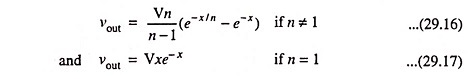
If the time constant of the circuit is very high i.e., RC is much greater than τ(n >> 1), the second term of the Eq. (29.16) is negligible compared to the first term except for very small values of time. Then

The above equation agrees with the way the circuit should behave for an ideal step voltage. The response of the High Pass RC Circuit for different values of n is depicted in Fig. 29.12.
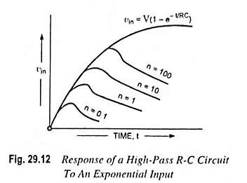
Near the origin of time, the output follows the input. Also, the smaller the circuit time constant, the smaller will be the output peak and narrower will be the pulse. The larger the circuit time constant, the larger will be the peak output but also the wider will be the pulse. A value of RC is chosen to provide the best compromise between these two conflicting characteristics for the particular application at hand. The choice is seldom critical.
Application:
R-C circuit with RC >> T is employed in R-C coupling of amplifiers where distortion and differentiation of waveform is to be avoided. R-C circuit with RC << T is employed to generate pips for triggering electronic circuits such as multivibrators, flip-flops etc.