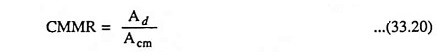
CMRR of Op Amp Formula (Common Mode Rejection Ratio):
One of the more common features of a differential amplifier is its ability to cancel out or reject certain types of undesired voltage signals. Such undesired signals are referred to as “noise” and may occur owing to voltages induced by stray magnetic fields in the ground or signal wires, as voltage variations in the voltage supply. Here the important point is that these noise signals are not the signals that are desired to be amplified in the differential amplifier. Their distinguishing feature is that the noise signal appears equally at both inputs of the circuit. It means that any undesired (or noise) signals that appear in polarity, or common to both input terminals, will be largely rejected, or cancelled out at the differential amplifier output. The signal that is to be amplified appears at only one input or opposite in polarity at both inputs. Now what is important to be considered is that, if undesirable noise does occur, up to what extent it is rejected out by the differential amplifier? A measure of this rejection of signals common to both inputs is referred to as the CMRR of Op Amp and a numerical value is assigned, which is called the common-mode rejection ratio (CMRR).
CMRR is defined as the ratio of differential voltage gain to common-mode voltage gain and it is given as

If a differential amplifier is perfect, CMRR would be infinite because in that case common-mode voltage gain Acm would be zero.
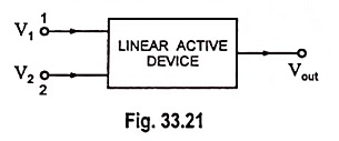
Figure 33.21 represents a linear active device with two input signals V1 and V2 and one output signal Vout, each measured with respect to ground. In an ideal differential amplifier the output signal Vout should be given as
![]()
where A is the gain of the differential amplifier.
Common to both the inputs will have no effect on the output voltage. However, in a practical differential amplifier, the output not only depends upon the difference signal Vd of the two input signals, but also upon the average level, called the common-mode signal Vcm where
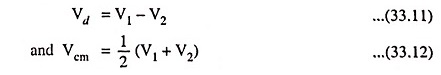
For example the output in the two cases having input signals of (V1 = +100 μV and V2 = -50 μV) and (V1 = +1,200 μV and V2 = +1050 μV) will not be exactly the same, even though the algebraic difference of two input signals Vd in both cases is the same i.e., 150 μV.
Now let the output voltage Vout in Fig. 33.21 be expressed as a linear combination of two input voltages as below
![]()
where A1 is the voltage gain for input V1 with V2 grounded and A2 is the voltage gain for the input V2 with V1 grounded.
But from Eqs. (33.11) and (33.12)
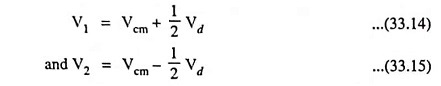
Substituting the values of V1 with V2 from above Eqs. (33.14) and (33.15) in Eq. (33.13) we have
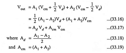
Here Ad is the voltage gain for the difference signal while Acm is the voltage gain for the common-mode signal.
The voltage gain Ad may be measured directly by selecting V1 = -V2 = 0.5 V so that Vd = 1 V and Vcm = 0 V. Under such conditions output voltage is Ad x (1 V) i.e., the output voltage equals Ad.
Similarly for measuring Acm, select V1 = V2 = 1 V, so that Vd = 0 and Vcm = 1 V. Under such conditions output voltage is Acm x (1 V) i.e., the output voltage equals Acm.
Thus, values of differential voltage gain Ad and common-mode voltage gain Acm can be determined simply by measurement of output voltage.
Having measured Ad and Acm for the amplifier, CMRR of Op Amp formula can be determined from the following relation
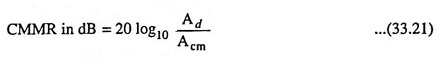
The value of CMRR of Op Amp can also be expressed in logarithmic terms as
From Eqs. (33.17) and (33.20) we have an expression for the output voltage in the following form
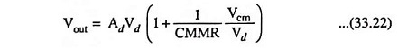
From above Eq. (33.22) it is seen that the amplifier should be designed so that CMRR is large in comparison to the ratio of common-mode signal to the difference signal (Vcm/Vd).
Even if both components of voltage Vcm and Vd exist at the inputs, the value of (1/CMMR Vcm/Vd) will be very small, for CMRR very large, and the output voltage will be almost equal to AdVd. It means that the output will be almost completely due to the difference signal with the common-mode input signals rejected or cancelled out.
As seen above, higher the value of CMRR, better is the performance of differential amplifier. Hence in practice the efforts are always to improve the CMRR of Op Amp.
For improvement of CMRR of Op Amp, it is necessary to reduce common mode gain Acm. The common mode gain Acm approaches zero, as the emitter resistance RE tends to ∞. This is because RE introduces a negative feedback in the common mode operation which reduces the common mode gain Acm. Thus higher the value of RE, lower is the value of Acm and higher is the value of CMRR of Op Amp. The differential gain Ad is not dependent on RE. But it is not practical to increase RE to a very high due to certain limitations such as (i) Large RE means higher biasing voltage to set the operating point Q of the transistors (ii) increase in overall chip area.
Hence, in practice, instead of increasing RE, various other methods are used which provide effect of increased RE without limitations. Such methods are (i) constant current bias method (ii) use of current mirror circuit.
The other method used is to increase the differential gain Ad and Ad can be increased by using active load.