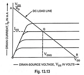
DC Load Line and Bias Point of FET Circuit:
The DC Load Line and Bias Point for a FET circuit is drawn upon the output characteristics of the device in exactly the same way as for a BJT circuit.
Consider the FET circuit and characteristics shown in Figs. 13.14 and 13.13 respectively.
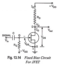
The drain-source voltage is given as
![]()
where VDD is the supply voltage and IDRD is the voltage drop across RD.
Consider the following two particular situations:
![]()
By joining these two points A and B, dc load line is obtained.
A dc bias point or quiescent point (Q-point) is selected on the FET dc load line. This point defines the dc conditions that exist in a circuit when no input signal is applied. The bias point is selected to provide maximum possible variations in output (drain-source) voltage when the drain current is varied by an input signal. In this case the positive-going and negative-going output voltage swings should be as closely equal as possible. Where maximum output voltage swing is not required, the bias point may be at any convenient position on the load line.
For the load line in Fig. 13.13, the bias conditions are VDD/2 and VDD/2RD.
![]()
For a FET amplifier, VDS must remain in the pinch-off region of the characteristics. This means that it must not be allowed to go below the level of the pinch-off voltage |VP| [in Fig. 13.8 (b)]. Thus, in the design of a FET bias circuit, the drain source voltage should always be a minimum of (-VP + 1) volts.
![]()
When an external bias voltage VGS is included, the pinch-off voltage for that bias level on the drain characteristics is (VGS – VP), where VP is the pinch-off voltage at VGS = 0 [Fig. 13.8 (b)]. Consequently, the minimum drain-source voltage may be reduced to
![]()
For the operation of FET as a switch, the device will either be biased off or on into the channel ohmic region of the drain characteristics.