FET Equivalent Circuit Model:
The complete FET Equivalent Circuit Model is shown in Fig. 11-5(a). It is seen that tilt source terminal is common to both input and out, so this is a common-source equivalent circuit. Resistor RGS between the gate and source terminals is the resistance of the reverse-biased gate-source junction, and Cgs is the junction capacitance. So, a signal applied to the input sees RGS in parallel with Cgs.
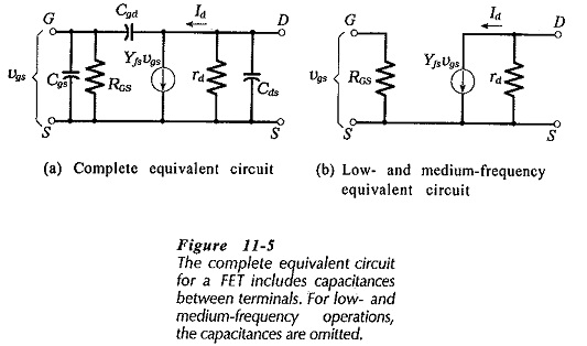
The output stage of the FET Equivalent Circuit Model is represented as a current source (Yfs vgs) supplying current to the drain resistance (rd). Yfs is the forward transfer admittance for the FET, and vgs is the ac signal voltage developed across the gate-source terminals, so the ac drain current is (Yfs vgs). The drain-source capacitance (Cds) appears in parallel with rd, and the gate-drain capacitance (Cgd) is shown connected between the input and output stages.
For low- and medium-frequency operations the capacitances can be neglected, and the equivalent circuit is then as shown in Fig. 11-5(b). This is the FET model (or equivalent circuit) normally used in ac circuit analysis.
Equivalent Circuit Parameters:
The parameters used in the FET Equivalent Circuit Model are already explained. As explained, RGS is a junction reverse resistance with a 109 Ω typical value for a JFET. Because its resistance is so high, RGS is often regarded as an open circuit. Instead of RGS being listed on a device data sheet, the gate-source reverse current is usually specified, and a value for RGS can be calculated from this quantity.
The forward transfer admittance (Yfs or gfs) varies widely for different types of FET. For a small-signal or switching JFET, Yfs typically ranges from 1000 μS to 5000 μS. For an E-MOSFET, Yfs might be 2.9 S.
The drain resistance (rd) shown in the FET Equivalent Circuit Model is the ac resistance offered between the drain and source terminals of the FET when operating in the pinch-off region of the drain characteristics. This quantity is usually defined in terms of an output admittance (Yos) which equals 1/rd. Typical values of rd range from 20 kΩ to 100 kΩ for a JFET.