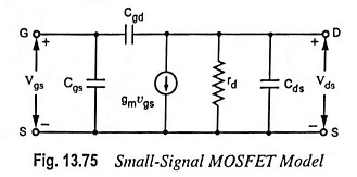
Small Signal Model of MOSFET:
If the small bulk resistances of the source and drain are neglected, the Small Signal Model of MOSFET and its equivalent circuit between terminals G (G1), S, and D is identical with that for the JFET and is as given in Fig. 13.75.
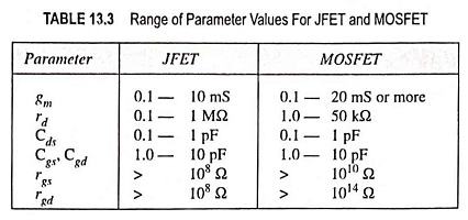
The transconductance and the interelectrode capacitances have comparable values for the two devices, as obvious from the figures given in Table 13.3. However, as indicated in Table 13.3, the drain resistance rd of the MOSFET is very much smaller than that of the JFET. It is also to be noted from Table 13.3 that the input resistance rgs and the feedback resistance rgd are very much larger for the MOSFET than for the JFET.
If the substrate terminal G2 is not connected to the source, the model of Fig. 13.75 must be generalized as follows :
Between node G2 and S, a diode D1 is added to represent the P-N junction between the substrate and the source. Similarly, a second diode D2 is included between G2 and D to account for the P-N junction formed by the substrate and drain.