Switching Characteristics of Power MOSFET:
Power MOSFET is an enhancement mode device modified to handle much large currents and voltages than a conventional MOSFET. Prior to the invention of the power MOSFETs, MOSFETs could not compete with the power ratings of larger BJTs. But now the power MOSFETs are better than the power BJTs in many applications requiring high load power.
As already explained, one main advantage of power MOSFETs is that they are inherently temperature stable and cannot go into thermal runaway. Another advantage of power MOSFETs is that they can be operated in parallel while power BJTs cannot.
In addition to above, Switching Characteristics of Power MOSFET have the advantage of switching a large current off faster than a BJTs can because a power MOSFET does not have minority carriers. They are 10 to 100 times faster than with comparable BJTs.
During cut-off the gate-to-source vgs is less than threshold value. To turn on, vgs is to be increased to well above the threshold value. The drain-to-source voltage must be less than vgs – VGST. The Switching Characteristics of Power MOSFET are influenced to a large extent by the internal capacitances of the device and the internal impedance of the gate drive circuit.
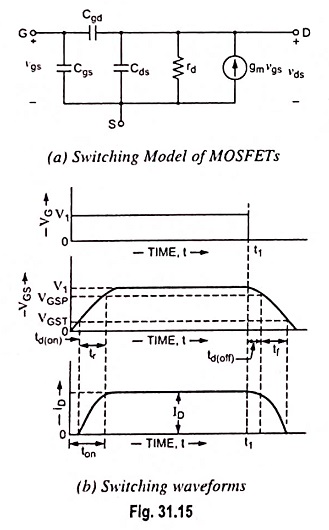
The Switching Characteristics of Power MOSFET is shown in Fig. 31.15(a). The three internal capacitances are gate-to-source capacitance Cgs, gate-to-drain capacitance Cgd and drain-to-source Cgd. During turning on Cgd and Cgs are to be charged through gate. This charging takes a finite time. So, the turn on cannot be instantaneous. Moreover, these capacitances are nonlinear and are not constant but dependent on dc bias voltage.
The typical switching waveforms of Power MOSFETs are shown in Fig. 31.15(b).
The turn-on delay td(on) is the time that is required to charge the input capacitance to threshold voltage level. The rise time tr is the gate charging time from the threshold level to the full-gate voltage VGSP. During rise time, drain current rises from zero to full-on current ID. Thus, the total turn-on time ton = td(on) + tr. The turn-on time can be reduced by using low-impedance gate-drive source.
As the MOSFET is the majority carrier device, turn-off process is initiated soon after removal of gate voltage at time t1. The turn-off delay time td(off) is the time required for the input capacitance to discharge from the overdrive gate voltage V1 to the pinch-off-region. VGS must decrease significantly before VDS begins to rise. The fall time, tf is the time that is required for the input capacitance to discharge from the pinch-off region to threshold voltage VGST. If VGS ≤ VGST, the transistor turns off. During fall time, drain current reduces from ID to zero.