Applications of FETs (Field Effect Transistors):
Applications of FETs – FET has a very high input impedance (100 MΩ in case of JFETs and 104 to 109 MΩ in case of MOSFETs), the major shortcomings of an ordinary transistor i.e., low input impedance with consequent of loading of signal source is eliminated in FET. Hence FET is an ideal device for use in almost every application in which transistors can be used.
- FETs are widely used as input amplifiers in oscilloscopes, electronic voltmeters and other measuring and testing equipment because of their high input impedance.
- Another applications of FETs are it is used in RF amplifiers in FM tuners and communication equipment’s for the low noise level.
- Another applications of FETs are it is used as voltage variable resistors (VVRs) in operational amplifiers and tone controllers etc. because it is a voltage controlled device.
- FETs are used in mixer circuits in FM and TV receivers, and communication equipment’s because of their low intermodulation distortion.
- FETs are used in low frequency amplifiers in hearing aids and inductive transducers because of the small coupling capacitors.
- Another applications of FETs are it is used in digital circuits in computers, LSI and memory circuits because of very small size.
Other applications of FETs are :
1. As An Analog Switch: FET as an analog switch is shown in Fig. 13.57 (a). When no gate voltage is applied to the FET i.e.,
VGS = 0, FET becomes saturated and it behaves like a small resistance usually of the value of less than 100 Ω and, therefore, output voltage becomes equal to
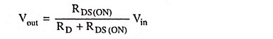
Since RD is very large in comparison to RDS (ON), Vout can be taken equal to zero.
When a negative voltage equal to VGS (OFF) is applied to the gate, the FET operates in the cutoff region and it acts like a very high resistance usually of some mega ohms. Hence output voltage becomes nearly equal to input voltage.
The circuit shown in Fig. 13.57 (a) is for a JFET shunt switch. Its equivalent circuit is shown in Fig. 13.57 (b) .
For normal operation, the ac input voltage must be a small signal, typically less than 100 mV. A small signal ensures that the JFET remains in ohmic region when the ac signal attains its positive peak value. Also RD is much greater than RDS to ensure hard saturation
![]()
When VGS is high, the JFET operates in the ohmic region and switch shown in Fig. 13.57 (b) is closed. Since RDS is much smaller than RD, vout is much smaller than vin. When VGS is low, the JFET cuts off and the switch shown in Fig. 13.57 (b) opens. In this case vout = vin. Thus, the JFET shunt switch either transmits the ac signal or blocks it.
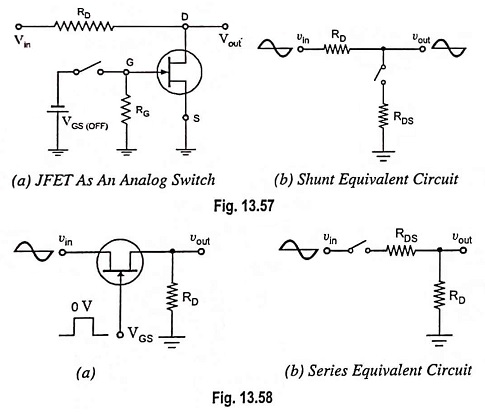
A JFET series switch with its equivalent circuit is shown in Fig. 13.58. When VGS is high, the switch is closed and the JFET is equivalent to a resistance of RDS. In this case, output is approximately equal to the input. When VGS is low, the JFET is open and vout is approximately zero.
2. Low Noise Amplifier: Noise is an undesirable disturbance superimposed on a useful signal. Noise interferes with the information contained in the signal; the greater the noise, the less the information. For instance, the noise in radio receivers develops crackling and hissing, which sometimes completely masks the voice or music. Similarly, the noise in TV receivers produces small white or black spots on the picture; a severe noise may wipe out the picture altogether. Noise is independent of the signal strength because it exists even when the signal is off.
Every electronic device produces certain amount of noise but FET is a device which causes very little noise. This is especially important near the front end of the receivers and other electronic equipment because the subsequent stages amplify front end noise along with the signal. If FET is used at the front end, we get less amplified noise (disturbance) at the final output.
Other circuits near the front end of receivers include frequency mixers and oscillators. JFETs-are often employed in VHF/UHF amplifiers, mixers and oscillators.
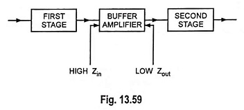
3. Buffer Amplifier: A buffer amplifier is a stage of amplification that isolates the preceding stage from the following stage. Source follower (common drain circuit) is used as a buffer amplifier. Because of the high input impedance and low output impedance a FET acts as an excellent buffer amplifier, as shown in Fig. 13.59. Owing to high input impedance almost all the output voltage of the preceding stage appears at the input of the buffer amplifier and owing to low output impedance all the output voltage from the buffer amplifier reaches the input of the following stage, even there may be a small load resistance.
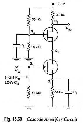
4. Cascode Amplifier: Circuit diagram for a cascode amplifier using FET is shown in Fig. 13.60. A common source amplifier drives a common gate amplifier in it.
Gain of common source amplifier,
![]()
RD will be equal to input resistance of the common gate amplifier.
Gain of common gate amplifier,
![]()
So overall gain of both FETs,
![]()
i.e., the cascode amplifier has the same voltage gain as a common source (CS) amplifier. The main advantage of cascode connection is its low input capacitance which is considerably less than the input capacitance of a CS amplifier. It has high input resistance which is also a desirable feature.
The low input capacitance is very significant with VHF and UHF signals. At these higher frequencies, the input capacitance becomes a limiting factor on the voltage gain. With a cascode amplifier, the low input capacitance allows the circuit to amplify higher frequencies than are possible with only a CS amplifier.
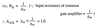
5. Chopper Amplifier: A direct-coupled amplifier can be built by leaving out the coupling and bypass capacitors and connecting the output of each stage directly to the input of the next stage. Thus, dc voltages are coupled, as are ac voltages. The major drawback of a direct coupling is drift, a slow shift in the final dc output voltage produced by minor variations in supply voltage, transistor parameters, and temperature.
The drift problem caused by direct coupling can be overcome by using chopper method in place of using direct coupling [Fig. 13.61 (a)]. Here the input dc voltage is chopped by a switching circuit, resulting in the square wave at the chopper output. The peak value of this square wave is equal to that of the input dc voltage VDC. Because the square wave is an ac signal, a conventional ac amplifier, one with coupling and bypass capacitors between the stages, can be used for amplification of the square wave. The coupling and bypass capacitors avoid the drift problem because they do not couple the drift. The amplified output can then be ‘peak detected’ to recover the amplified dc signal.
Square wave is applied to the gate of a FET analog switch to make it operate like a chopper, as illustrated in Fig. 13.61 (b). The gate square wave is negative-going, swinging from 0 V to at least VGS (OFF). This alternately saturates and cuts off the JFET. Thus output voltage is a square wave varying from +VDC to zero volt alternately.
If the input signal is a low-frequency ac signal, it gets chopped into the ac waveform as shown in Fig. 13.61 (c). This chopped signal can now be amplified by an ac amplifier that is drift free. The amplified signal can then be peak detected to recover the original input low frequency ac signal. Thus both dc and low frequency ac signals can be amplified by using a chopper amplifier.
JFET can use either a shunt switch, as shown in Fig. 13.61 (b) or a series switch.
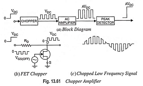
6. Multiplexer: Multiplexer means “many into one”. An analog multiplexer, a circuit that steers one or more of the input signals to the output line, is shown in Fig. 13.62. Each JFET acts like a series switch. The control signals (V1, V2 and V3) turn the JFETs on and off. When a control signal is high, its input signal is transmitted to the output. When the control signals (V1, V2 and V3) are more negative than VGS (OFF) all input signals are blocked. By making any control voltage equal to zero, one of the inputs can be transmitted to the output. For instance, when V1 is zero, the signal obtained at the output will be sinusoidal. Similarly when V2 is zero, the signal obtained at the output will be triangular and when V3 is zero, the output signal will be square-wave one. Normally, only one of the control signals is zero.
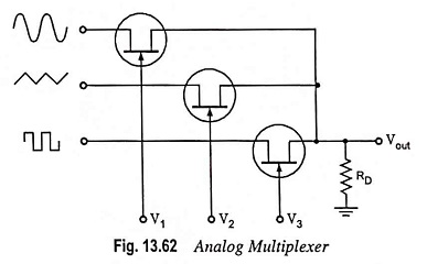
7. Current Limiter: JFET current limiting circuit is shown in Fig. 13.63. It is used for protection against excessive current. For instance let the normal load current be 1.25 mA. If IDSS = 8 mA and RDS (ON) = 160 Ω, then a normal load current of 1.25 mA will cause a voltage drop VDS of 1.25 x 10-3 x 160 = 0.2 V i.e., JFET will operate in the ohmic region.
Almost all the supply voltage, therefore, appears across the load. When the load current tries to increase to an excessive level (may be due to short circuit or any other reason), the excessive load current forces the JFET into active region, where it limits the current to 8 mA. The JFET now acts as a current source and prevents excessive load current.
A manufacturer can tie the gate to the source and package the JFET as a two terminal device. This is how constant-current diodes are made. Such diodes are also called current-regulator diodes.
8. Phase-Shift Oscillators: JFET can incorporate the amplifying action as well as feedback action. It, therefore, acts well as a phase shift oscillator. The high input impedance of FET is especially very valuable and the applications of FETs is used in phase-shift oscillators in order to minimize the loading effect.