Field Effect Transistors (FETs) Interview Questions and Answers:
1. What is the major difference between a bipolar and a unipolar device ?
Ans. In a bipolar device, current conduction is by both majority carriers and minority carriers (both by holes as well as electrons), such as in a case of BJT. On the other hand, in a unipolar device, the current conduction is by only one type of majority carriers (either by electrons or by holes), such as in case of FET.
2. Explain why BJTs are called bipolar devices while FETs are called unipolar devices.
Ans. In ordinary transistors, current conduction is by both majority carriers and minority carriers (both by holes as well as electrons) and, therefore, these are called bipolar transistors. In field-effect transistors current conduction is by only one type of majority carriers (either by electrons or by holes) and, therefore, these are called unipolar transistors.
3. Define “current-controlled device” and “voltage-controlled device”.
Ans. A current-controlled device is one in which a current defines the operating conditions of the device, whereas a voltage-controlled device is one in which a particular voltage defines the operating conditions.
4. Why is terminology “field effect” appropriate for this terminal device ?
Ans. The device is called field-effect transistor (FET) because the drain current (output current) is controlled by the effect of extension of the field associated with the depletion region developed by the reverse bias at the gate.
5. Why IG is effectively zero ampere for a JFET transistor ?
Ans. The gate channel junction in a JFET is a P-N junction and since it is normally reverse biased, a minority charge carrier current flows. This is gate-source cutoff current, known as gate reverse current. So the gate current, IG can be said to be effectively zero ampere.
6. What do you understand by terms channel and drain in JFET ?
Ans. Channel. The region between the source and drain, sandwiched between the two gates is called the channel and the majority carriers move from source to drain through this channel.
Drain. The terminal, through which the majority carriers leave the channel, is called the drain terminal D and the conventional current leaving the channel at D is designated as ID.
7. Why the channel of a JFET is never completely closed at the drain end ?
Ans. If the channel is completely closed in JFET, then there will be no drain current, so there will be no voltage drop along the channel length and amount of reverse bias will become uniform and wedge-shaped depletion region will become rectangular one.
8. How is drain current controlled in a JFET?
Ans. In a JFET drain current is controlled by controlling the reverse bias given to its gate (i.e., VGS).
9. What is meant by drain characteristic of FETs?
Ans. The curve drawn between drain current and drain-source voltage with gate-to-source voltage as the parameter is called the drain characteristic.
10. What happens to the drain current of a P-channel JFET when a positive voltage is applied on its gate?
Ans. Whenever the positive voltage is applied to the gate of P-channel JFET, the depletion region width increases because of which channel is narrowed, the resistance is increased and drain current is reduced.
11. What is meant by transfer characteristic of FETs?
Ans. The curve drawn between drain current and gate-source voltage for a given value of drain-source voltage is called the transfer characteristic.
12. Define pinch-off voltage for a JFET.
Ans. The negative of the value of drain-source voltage at which channel is pinched off (i.e., all the free charges from the channel get removed) is called the pinch-off voltage.
13. What are the parameters that control the pinch-off voltage of JFET?
Ans. Parameters that control the pinch-off voltage of JFET are electron charge, donor/acceptor concentration density, permittivity of channel material and half width of channel bar.
14. Why FET is called the voltage controlled device?
Ans. In a FET, drain current is controlled by the effect of the extension of the field associated with the depletion region developed by the reverse bias on the gate, so it is called a voltage controlled device.
15. What is Shockley equation?
Ans. Drain current in the pinch-off region of JFET is given by the equation, known as Shockley equation.
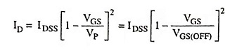
where ID is the drain current at a given gate-source voltage VGS, IDSS is the drain current with gate shorted to source and VGS is the gate-source cutoff voltage.
16. What is meant by gate-source cutoff voltage?
Ans. The gate-source bias voltage required to reduce the drain current to zero is designated the gate-source cutoff voltage VGS(OFF). It is equal to pinch-off voltage VP.
17. What is meant by saturation region?
Ans. The region of drain characteristic of a FET in which drain current remains fairly constant is called the saturation or pinch-off region.
18. What is meant by drain-source saturation current lDSS?
Ans. The drain current in pinch-off or saturation region with zero gate-source voltage (VGS = 0) is referred to the drain-source saturation current lDSS.
19. What is physical significance of high input impedance of an FET?
Ans. Input circuit of an FET (gate to source) is reverse biased and the input gate current is very small (of the order of few nA), so the input impedance is very high. It permits high degree of isolation between the input and output circuits.
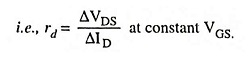
20. What is dynamic resistance of a JFET?
Ans. The ratio of change in drain-source voltage to change in drain current at a given gate-source voltage is known as ac drain resistance or dynamic resistance rd
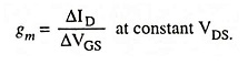
21. What is meant by transconductance with reference to JFET?
Ans. The control that gate-source voltage has over the drain current is measured by the transconductance of a JFET. It may be defined as the ratio of change in drain current to the change in gate-source voltage for a given value of drain-source voltage i.e.,
22. In practice, the voltage divider bias is less effective with JFET than BJT. Why?
Ans. This is because in BJT, VBE = 0.7 V (silicon) with only minor variations from one transistor to another transistor. But in a JFET, the VGS can vary several volts from one JFET to another.
23. Why is CS JFET amplifier most widely used?
Ans. The common source configuration is the most widely employed configuration. It is because this configuration provides high input impedance, good voltage gain and moderate output impedance.
24. Give features and applications of CS amplifier.
Ans. The features of CS JFET amplifier are: (i) high input impedance, (ii) moderate output impedance, (iii) high voltage gain and has 180° phase shift between the input and output.
It is used as it preamplifier in audio circuits, as a voltage amplifier and in the radio and TV amplifier circuits.
25. Why common drain (CD) amplifier is called a source follower?
Ans. The output voltage at the FET source terminal follows the variations in signal voltage applied to the gate, therefore, the common drain circuit is also known as a source follower.
26. Give features of CD JFET amplifier.
Ans. The CD JFET amplifier has features of (i) very high input impedance, (ii) very low output impedance, (iii) low (≈ 1) voltage gain and (iv) no phase inversion.
27. Give features CG JFET amplifier.
Ans. The CG JFET amplifier has features of (i) low input impedance, (ii) high output impedance, (iii) high voltage gain and no phase inversion.
28. What is the basic difference between JFET and MOSFET?
Ans. In a junction field-effect transistor (JFET) the gate voltage controls the depletion width of a reversed biased P-N junction. A metal semiconductor field-effect transistor (MESFET) is the same basic device except that the P-N junction is replaced by a Schottky barrier rectifying junction. Metal-insulatorsemiconductor field-effect transistor (MISFET) is one in which the metal gate electrode may be separated from the semiconductor by an insulator. The metal-oxide semiconductor field-effect transistor (MOSFET) is a special type of MISFET which makes use of an oxide layer as insulator.
29. Why is MOSFET called sometimes IGFET?
Ans. MOSFET is constructed with the gate terminal insulated from the channel so it is sometimes called insulated gate FET (or IGFET).
30. Write the types of MOSFET and their two major differences.
Ans. MOSFETs are of two types namely (i) enhancement type MOSFET or E-MOSFET and (ii) depletion type MOSFET or DE-MOSFET. In the depletion-mode channel is physically constructed and a current flow between drain and source due to voltage applied across the drain-source terminals. The enhancement MOSFET structure has no channel formed during its construction. Voltage is applied to the gate, in this case, channel of charge carriers is developed, so that a current results when a voltage is applied across the drain-source terminals.
Depletion mode devices are normally on when the gate-source voltage VGS = 0, whereas the enhancement-mode devices are normally off when VGs = 0.
31. In the linear region operation of MOSFET drain current decreases as the temperature increases. Explain.
Ans. In the linear operation of MOSFET, with the increase in temperature the mobility of the charge carriers decreases and therefore conductivity of the MOSFET reduces. Thus the drain current reduces with the increase in temperature.
32. What is meant by threshold voltage?
Ans. The minimum value of gate-to-source voltage VGS that is required to form the inversion layer is termed the gate-to-source threshold voltage VGST.
33. Why MOSFETs are never connected or disconnected in the circuit when power is ON?
Ans. If a MOSFET is connected or disconnected in circuit while the power is ON, transient voltages caused by inductive kickback and other effects may exceed VGS(max) and thus wipe out the MOSFET.
34. Name the factors which make the JFET superior to BJT?
Ans. The high input impedance, low output impedance and low noise level make JFET far superior to the BJT.
35. Why enhancement mode MOSFETs are preferred over the depletion mode ones in the fabrication of integrated circuits?
Ans. Since the conductivity of the channel is enhanced by the positive bias given to the gate in case of enhancement mode MOSFETs, the E-MOSFETs are preferred over the DE-MOSFETs in the fabrication of ICs.
36. In communication electronics, why JFET RF amplifier is used in a receiver instead of BJT amplifier ?
Ans. The reasons for using JFET RF amplifier in receiver instead of BJT amplifier are:
- The noise level of JFET is very low.
- The antenna of the receiver receives a very weak signal that has an extremely low amount of current. Since JFET is a voltage controlled device, it will respond to low current signal provided by the antenna.
37. Give the features of a power MOSFET.
Ans. Power MOSFET is a unipolar and voltage controlled device and has positive temperature coefficient of resistance, more conduction loss in higher voltage rating and much more linear transfer functions. Power MOSFET has smaller switching losses but its on-resistance and conduction losses are more. So for higher frequency applications, power MOSFET is the obvious choice.