Differential Amplifier Circuit using Transistors:
The Differential Amplifier Circuit using Transistors is widely applied in integrated circuitry, because it has both good bias stability and good voltage gain without the use of large bypass capacitors. Differential amplifiers can also be constructed as discrete component circuits.
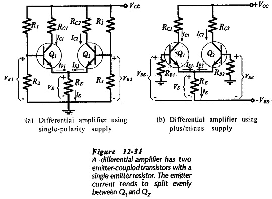
Figure 12-31(a) shows that a basic Differential Amplifier Circuit using Transistors consists of two voltage divider bias circuits with a single emitter resistor. The circuit is also known as an emitter-coupled amplifier, because the transistors are coupled at the emitter terminals, If transistors Q1 and Q2 are assumed to be identical in all respects, and if VB1 = VB2, then the emitter currents are equal, and the total emitter current is,
Like the emitter current in a single-transistor voltage divider bias circuit, IE in the differential amplifier remains virtually constant regardless of the transistor hFE value. This results in, IE1, IE2, IC1, and IC2 all remaining substantially constant, and the constant collector current levels keep VC1 and VC2 stable. So, the differential amplifier has the same excellent bias stability as a single-transistor voltage divider bias circuit.
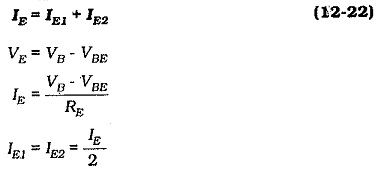
The circuit of a Differential Amplifier Circuit using Transistors using a plus-minus supply is shown in Fig. 12-31(b). In this case, the voltage across the emitter resistor is (VEE – VBE), as illustrated,
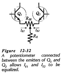
The base resistors (RB1 and RB2) are included to bias the transistor bases to ground while offering an acceptable input resistance to a signal applied to one of the bases. The transistor emitter currents (IE1 and IE2) are exactly equal only if the devices are perfectly matched. To allow for some differences in transistor parameters, a small-value potentiometer (REE) is sometimes included between the emitters, ( see Fig. 12-32). Adjustment of REE increases the resistance in series with the emitter of one transistor, and reduces the emitter resistance for the other transistor. This reduces the IE for one transistor and increases it for the other, while the total emitter current remains constant.
AC Operation:
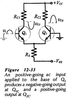
Consider what happens when the at input voltage (vi) at the base of Q1 is positive-going, as illustrated in Fig. 12-33. Q1 emitter current (IE1) increases. Also, IE2 decreases, because the total emitter current (IE1 + IE2) remains constant. This means that IC1 increases and IC2 decreases, and consequently, VC1 falls and VC2 rises, as shown. So, the ac output voltage at Q1 collector is in anti-phase to vi at Q1 base, and the output at Q2 collector is in phase with vi.
Voltage Gain:
The voltage gain of a single-stage amplifier with an unbypassed emitter resistor and no external load is given by
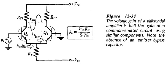
Referring to Fig. 12-34, it is seen that the resistance looking into the emitter of Q2 is hib, so hib||RE behaves like an unbypassed resistor in series with the emitter of Q1. Neglecting RE because it is very much larger than hib, the voltage gain from the base of Q1 to its collector is,
this reduces to,
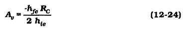
Equation 12-24 gives the voltage gain from one input terminal to one output of a differential amplifier. It is seen to be half the voltage gain of a similar single-transistor CE amplifier with RE bypassed; but note that the differential amplifier requires no bypass capacitor. This is an important advantage, because bypass capacitors are usually large and expensive.
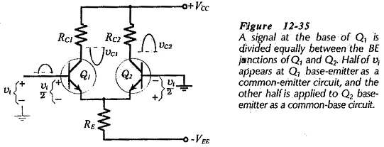
Another way to contemplate the operation of the Differential Amplifier Circuit using Transistors is to think of the input voltage being equally divided between Q1 base-emitter and Q2 base-emitter. This is illustrated in Fig. 12-35 where it is seen that (for a positive-going input) vi/2 is applied positive on the base of Q1, while the other half of vi appears positive on the emitter of Q2. Thus, for vi at Q1B, transistor Q1 behaves as a common-emitter circuit, and because Q2 receives the input at its emitter, Q2 behaves as a common-base circuit. Consequently,
Input and Output Impedances:
The input impedance at the base of a CE circuit with an unbypassed emitter resistor is,
![]()
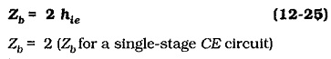
Referring to Fig. 12-34, the differential amplifier has. hib||RE as an unbypassed resistor in series with the emitter of Q1. Neglecting RE (because RE ≫ hib). The input resistance at Q1B is,
![]()
This reduces to,
Note that there are usually bias resistors in parallel with Zb, so that the circuit input impedance is
![]()
As in the case of CE and CB circuits, the output impedance at the transistor collector terminals is given by
![]()
DC Amplification:
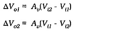
When one transistor base is grounded in a Differential Amplifier Circuit using Transistors, and an input is applied to the other one, as already discussed, vi is amplified to produce the outputs at the collector terminals. In this case vi is the voltage difference between the two base terminals. Figure 12-36 shows a differential amplifier with dc input voltages Vi1 and Vi2 applied to the transistor bases. If the voltage, gain from the base to the collector is Av, the dc voltage changes at the collectors are;
It is seen that the differential amplifier can be employed as a direct-coupled amplifier, or dc amplifier. The term difference amplifier is also used for this circuit.
Design Calculations:
Design procedures for a Differential Amplifier Circuit using Transistors are similar to those for voltage divider bias circuits. Because there is no bypass capacitor in a differential amplifier, one of the coupling capacitors determines the circuit lower cutoff frequency (f1). The capacitor with the smallest resistance in series with it is normally the largest capacitor, and in the case of a differential amplifier this is usually the input coupling capacitor. So, the input coupling capacitor determines the circuit lower cut-off frequency.
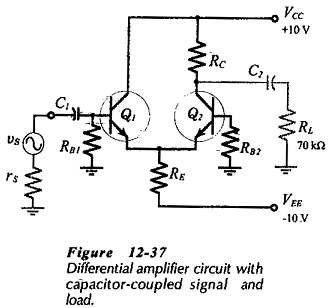
Consider the capacitor-coupled differential amplifier in Fig. 12-37. The circuit uses a plus-minus supply, and a single collector resistor (RC). No output is taken from Q1 collector, so there is no need for a collector resistor. RC is selected in the usual way for a small-signal amplifier; RC ≪ RL. The collector-emitter voltage should be a minimum of 3 V, as always. Then, IC is calculated from RC and the selected voltage drop across RC.
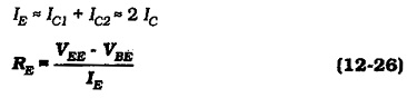
The total emitter current is determined as,
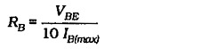
The base bias resistors are determined by,
As discussed, capacitor C1 sets the lower cutoff frequency. So.
![]()
and C2 is determined by,
![]()