Important Points Regarding Working of Transistors:
The noteworthy points regarding working of transistors are summarized below.
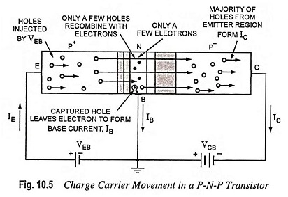
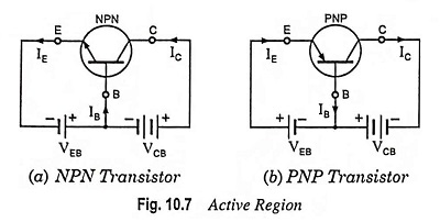
1. Current conduction in N-P-N transistor is by electrons and the conventional current flow will be in the opposite direction. Current conduction in P-N-P transistor is by holes but in external leads, the current conduction will be by flow of electrons.
2. The collector current lC is always less than emitter current lE, being the difference of emitter current lE and base current lB.
3. The base current is only a small fraction (usually 5%) of emitter current.
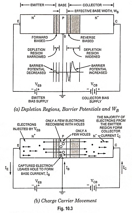
4. As a standard convention, all the currents entering into the transistor are considered to be positive. Conversely currents that flow out of the transistor are taken to be negative. It means that if the actual conventional current flows in the outward direction, a negative sign is included along with its magnitude. Thus in an N-P-N transistor, the emitter current lE is to be taken negative because it flows out of the transistor [Figs. 10.3 and 10.7 (a)] while both the base current lB and collector current IC are to be taken positive because they flow into the transistor. Similarly in a P-N-P transistor IE is to be taken positive and both base current IB and collector current IC are to be taken negative [Figs. 10.5 and 10.7 (b)]. However, to avoid confusion, the actual direction of flow of current is indicated in the diagrams.
5. Emitter-base junction is always forward biased and collector-base junction is always reverse biased for active region of operation.
6. The input circuit (i.e., emitter-base junction), because of forward bias, offers low resistance and so needs usually very small bias (approximately 0.7 V for Si and 0.3 V for Ge). The output circuit (i.e., collector-base junction), because of reverse bias, offers high resistance and, therefore, needs much higher bias (3 to 20 V).
7. Transistor transfers the input signal from a low resistance circuit to a high resistance circuit, therefore, it is called the TRANsfer reSISTOR (TRANSISTOR).
8. Since both of the charge carriers (holes as well as electrons) are involved in current flow through a transistor (may be either P-N-P or N-P-N), these devices are sometimes called the bipolar junction transistors (BJTs).
9. Although, it is said that a transistor is a device with two PN diodes connected back to back, but it does not mean that two discrete diodes connected back to back, as shown in Fig. 10.10, can work as a transistor. In such a case, each diode has two equally doped regions, so that the overall circuit has four equally doped regions. This would not work as base region is not the same as in a transistor.
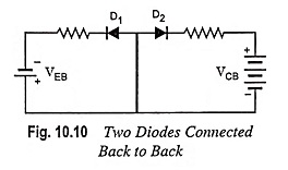
The key to the Working of Transistors action is the lightly doped thin base between the heavily doped emitter and moderately doped collector.
In an N-P-N transistor, the free electrons passing through the base to the collector region have a short lifetime. As long as the base is thin, the free electrons can reach the collector. But in case of two discrete back to back connected diodes there are four doped regions instead of three and there is nothing that resembles a thin base region between an emitter and a collector.
Hence two discrete diodes connected back to back can never work as a transistor.
10. The choice of N-P-N transistor is made more often because majority charge carriers are electrons whose mobility is much more (almost double) than that of holes.