Microwave Transistors:
Silicon bipolar transistors were first on the microwave scene, followed by GaAs field-effect transistors. Indeed, FETs now have noticeably lower noise figures, and in the C band and above they yield noticeably higher powers. A description of Microwave Transistors constructions and a discussion of their performance now follow.
Transistor Construction:
The various factors that contribute to a maximum high-frequency performance of microwave transistors are complex. They include the already mentioned requirement for high voltages and currents, and two other conditions. The first of these is a small electrode area to reduce interelectrode capacitance. The second is very narrow active regions to reduce transit time.
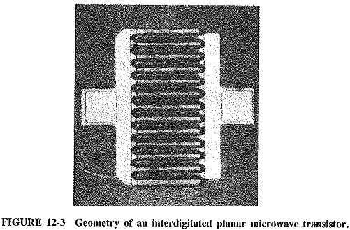
For bipolar transistors, these requirements translate themselves into the need for a very small emitter junction and a very thin base. Silicon planar transistors offer the best bipolar Microwave Transistors performance. Fabrication difficulties, together with the excellent performance of GaAs FETs, have prevented the manufacture of GaAs bipolars. Epitaxial diffused structures are used, giving a combination of small emitter area and large emitter edge. The first property gives a short transit time through the emitter, and the second a large current capacity. The interdigitated transistor, shown in Figure 12-3, is by far the most common bipolar in production. The transistor shown has a base and emitter layout that is similar to two hands with interlocking fingers, hence its name. The chip illustrated has overall dimensions (less contacts) of about 70 X 70 μm; the emitter contact is on the left, the base on the right and the collector underneath. The thickness of each emitter (and base) “finger” in the transistor shown is 0.5 μm. This yields values of fmax in excess of 20 GHz; 0.25-μm geometries have been proposed.
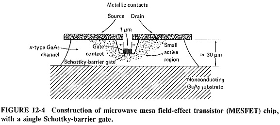
The most common microwave FET uses a Schottky-barrier gate. Figure 12-4 demonstrates why this device is also known as a MESFET. The cross section shows it to be of mesa construction. The top metallic layer has been etched away, as has a portion of the n-type GaAs semiconductor underneath. The metallic Schottky-barrier gate stripe is deposited in the resulting groove. It has a typical length of 1 μm (the normal range is 0.5-3 μm). The width of the gate is not shown in the cross section; 300-2400 μm is a typical range. Dual-gate GaAs FETs are also available, in which the second gate may be used for the application of AGC in receiver RF amplifiers. It should be mentioned that values of fmax in excess of 100 GHz are currently achievable.
Packaging and circuits:
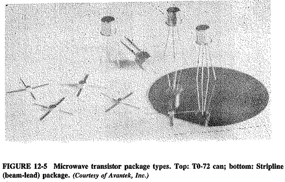
Two typical methods of packaging microwave transistors chips are. shown in Figure 12-5, The Avantek stripline package at the bottom has a body thickness of 1 mm and a diameter just under 5 mm. The TO-72 can at the top has a 7 1/2-mm diameter and much the same height. The TO-72 package is available for frequencies up to about 2 GHz, especially for silicon bipolar transistors. The stripline packages are used for higher frequencies, up to about 30 GHz, for bipolars or FETs. For still-higher frequencies or large bandwidths, the transistor chips are bonded directly to the associated circuitry.
Microwave Integrated Circuits:
Because of the inherent difficulties of operation at the highest frequencies, MICs took longer to develop than integrated circuits at lower frequencies. However, by the mid-1970s, hybrid MICs had become commercially available, at first with sapphire substrates and subsequently with (insulator) gallium arsenide substrates. In these circuits, thick or thin metallic film was deposited onto the substrate, and the passive components were etched onto the film, while the active components, such as transistors and diodes, were subsequently soldered or bonded onto each chip. In the early 1980s, however, monolithic MICs became commercially available. In these circuits, all the components are fabricated on each chip, using metallic films as appropriate for passive components and injection doping of the GaAs substrate to produce the requisite diodes and FETs. In view of the size reduction initially available from monolithic MICs, it appeared at first that they would completely take over the field, but significant improvements were made in hybrid circuits, with a consequent resurgence of their use. It would appear that the two types will be used side by side for the foreseeable future.
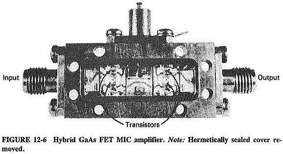
A typical hybrid MIC amplifier is illustrated in Figure 12-6. This is an Avantek miniature GaAs FET hybrid MIC, with overall dimensions (including connectors and dc power feedthrough) of about 40 X 20 X 4 mm—its volume is thus under 0.2 in3. The two-stage amplifier produces an output of 10 mW, with a gain of 9 dB and a noise figure of 8 dB, over the very wide frequency range of 6 to 18 GHz. It is seen that the two modules on either side of center are identical balanced amplifiers, with the two transistors located above each other in the middle of each module as indicated. In a working amplifier, a lid is welded on, dry nitrogen is pumped in, and the amplifier is hermetically sealed.
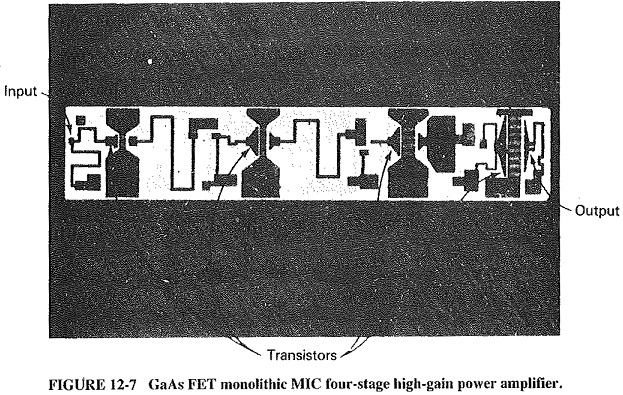
A Texas Instruments monolithic MIC chip is shown in Figure 12-7. This is a high-gain four-stage GaAs FET power amplifier developed for satellite communications. Although the chip measures only 1 X 5.25 X 0.15 mm, it produces an output of 1.3 W at 7.5 GHz, with a good frequency response from 6.5 to 8 GHz and an efficiency of 30 percent; the gain is 32 dB. The gate widths range from 300 μm for the input FET to 2400 μm for the output FET. Silicon nitride capacitors are used, and a fair amount of gold plating is used to reduce resistance.
Performance and Applications of Microwave Transistors and MICs:
The power and noise capabilities of microwave transistors and MICs have been improving spectacularly over more than a decade, with good improvements in bandwidth and efficiency over the same period.
Bipolar transistors are available for frequencies up to about 8 GHz, where power devices produce up to about 150 mW output, while low-noise transistors have noise figures of the order of 14 dB. Neither is as good as the corresponding figure for GaAs FETs. However, bipolars do very well at lower microwave frequencies: transistors such as the Avantek ones shown in Figure 12-5 produce noise figures as low as 2.8 dB at 4 GHz and 1.8 dB at 2 GHz, and power bipolars can produce over 1 W per transistor at 4 GHz.
GaAs FETs are available, as discrete transistors and/or MICs, right through the Ka band (26.5 to 40 GHz) and arc becoming available for higher frequencies. Powers of several watts per transistor are available up to 15 GHz, and hundreds of milliwatts to 30 GHz. Noise figures below 1 dB are attainable at 4 GHz and are still only about 2 dB at 20 GHz. The noise figures of amplifiers, be they bipolar or FET, are not as good as those of individual transistors. The major reason for this is the low gain per stage, typically 5 to 8 dB at X band (8 to 12.5 GHz).
As has been mentioned, FETs have the advantage over bipolars at the highest frequencies because they are able to use GaAs, which has a higher ion mobility than silicon. They also have higher peak electron velocities, the two advantages providing a faster transit time and lower dissipation. FETs are thus able to work at higher frequencies, with higher gain, lower noise and better efficiency. Other semiconductor materials currently being investigated as potentially useful at microwave frequencies, because of possible advantages in electron mobility and drift velocity over gallium arsenide, include gallium-indium arsenide (GalnAs).
With such excellent performance, transistor amplifiers (and oscillators) have found many microwave applications, especially as their prices have fallen. The advantages of transistors over other microwave devices include long Shelf and working lives, small size and electrode voltages, and low power dissipation together with good efficiencies, of the order of 40 percent. The noise figures and bandwidths are also excellent. Computer control of design and manufacture has resulted in good reliability and , repeatability of characteristics for both field-effect and bipolar transistors.
Low-noise transistor amplifiers are employed in the front ends of all kinds of microwave receivers, for both radar and communications. That is, unless the requirement is for extremely low noise, in which case transistors are used to amplify the output of more exotic RF amplifiers (treated later in this chapter). The application for microwave power transistors is as power amplifiers or oscillators in a variety of situations. For example, they serve as output stages in microwave links, driver amplifiers in a wide range of high-power transmitters (including radar ones), and as output stages in broadband generators and phased array radars.