Base Spreading Resistance:
With two depletion layers penetrating the base, the base holes are confined to the thin region of P-type semiconductor illustrated in Fig. 10.12. The resistance of this thin region (or section) is called the base spreading resistance rbb′. With the increase in reverse bias VCB on the collector diode, the width of the P-section is reduced, which is equivalent to an increase in rbb′.
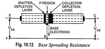
The recombination current in the base IB must flow through rbb′. When it does so it causes a voltage drop. The value of base spreading resistances rbb′ depends upon the width of the P-section as well as doping of the base. In rare case rbb′ may be as high as 1,000 Ω. Typically, it is in the range of 50-150 Ω. The effects of rbb′ are important in high-frequency circuits. At low frequencies rbb′ usually has little effect and so it is ignored.