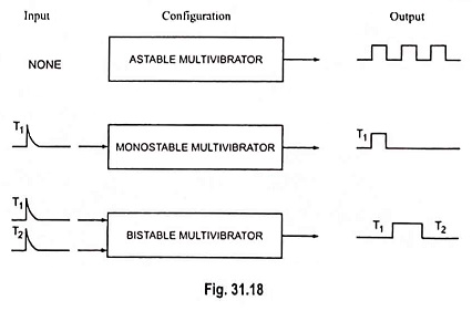
Monostable Multivibrator – Operation, Types and Application:
Monostable multivibrator is a two-stage amplifier with two states—one stable state and another quasi-stable state. The circuit has two transistors Q1 and Q2, one being in the offstate, say Q1, and the other, Q2, in the on state preferably in saturation. These transistors remain in this state for ever and only on the application of trigger, the multivibrator goes into the quasi-stable state, i.e., Q1 is on and Q2 is off. The circuit remains in the quasi-stable state for a period determined by the circuit components and then returns to its initial stable state, i.e., Q1 is off and Q2 is on. Thus, this circuit generates a pulse of duration T.
Types of Monostable Multivibrators:
- Collector-coupled monostable multivibrator
- Emitter-coupled monostable multivibrator.
1. Collector Coupled Monostable Multivibrator:
The circuit arrangement of a collector-coupled monostable multivibrator is shown in Fig. 31.24.
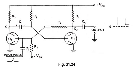
It consists of two similar transistors Q1 and Q2 with equal collector resistances R3 and R4 (i.e., R3 = R4). The circuit is designed for operation with transistor Q2 normally conducting and transistor Q1 cut off. The output of transistor Q1 is coupled to the base of transistor Q2 via capacitor C1. However, the other coupling is direct one through base resistor R1. Transistor Q2 is forward biased by power supply VCC and base resistor R2 and remains saturated in stable state. Operation in this stable state is ensured if the biasing resistor R2 is selected to permit sufficient base current in transistor Q2 for operation in saturation region. Transistor Q1 is reverse biased by power supply VBB and resistor R5 remains cut off in the stable state. The input pulse is applied through capacitor C2. The output may be taken from either of the transistors Q1 or Q2.
Operation:
When the power supply is switched on but with no input pulse applied, transistor Q2 is on and is operating in its saturation region. It is being forward biased by supply VCC and base resistor R2. The collector of transistor Q2 is virtually at ground potential. The base of transistor Q2 is 0.7 V above ground potential because of the forward-bias of base-emitter junction. This is illustrated in Figs. 31.25(a) and 31.25(b).
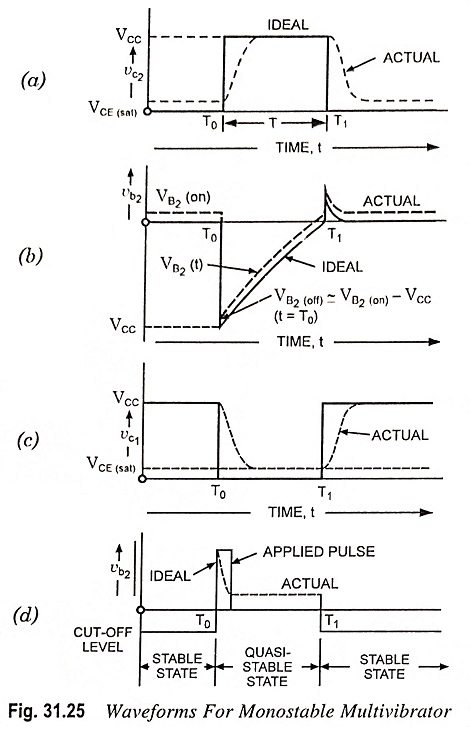
Transistor Q1 is cut off being reverse biased by supply VBB and resistor R5. Its base resistor R1 is connected to the collector of transistor Q2, which is at zero potential. Thus collector resistor R3 is completely disconnected from the grounded emitter of transistor Q1 and is free to carry current to charge capacitor C1. Since capacitor C1 is connected to the base of transistor Q2, which is close to ground potential, it will charge up almost to the supply voltage VCC. The polarity of the charge on capacitor C1 is plus (+) on the left and minus (–) on the right, as shown.
When a positive trigger pulse of short duration and sufficient magnitude is applied to the base of transistor Q1 through capacitor C2, it (input pulse) overrides the reverse bias of emitter-base junction of transistor Q1 and gives it a forward bias. Thus transistor Q1 starts conducting and the potential of collector of transistor Q1 comes down to ground. Since charge on capacitor C1 cannot disappear instantly, the voltage across the capacitor plates is maintained. With the positive side of the capacitor C1 pulled down to zero volt by transistor Q1, the negative side goes to a voltage far below ground potential. Thus a negative bias is applied to the base of transistor Q2 and transistor Q2 is cut off. The collector of transistor Q2 rises toward VCC and is now capable of supplying base current to transistor Q1 through its base resistor R1. Thus transistor Q1 remains turned on even after the positive spike from the transistor Q1 is removed.
As time passes charging current flows onto the plates of capacitor C1. The flow path is down through R2, through capacitor C1 and through collector to emitter of Q1 into ground. As can be seen, this path seeks to charge capacitor C1 to the opposite polarity, what happens is that the voltage across capacitor C1 gets reduced. When the voltage across the capacitor crosses through zero and attains 0.7 V in the opposite polarity, as shown in Fig. 31.25 (b), it bleeds a small amount of current into the base of transistor Q2. This small base current causes collector current to flow in transistor Q2, lowering its collector voltage. The reduced collector voltage causes a reduction in base current to transistor Q1. This in turn causes a reduction in collector current of Q1. The Q1 collector voltage rises slightly, thereby raising the base of Q2 higher yet. This action is regenerative; once it begins, it avalanches. In the end, transistor Q2 is saturated once again and transistor Q1 is cut off. Thus the circuit reverts back to its original stable state. The circuit remains in this state until another triggering pulse causes the circuit to switch over the state and the other cycle repeats itself.
The width of the output pulse is determined by the time constant of C1R2. The multivibrator generates one output pulse for every input trigger pulse and that is why it is sometimes called the one shot multivibrator. The width or duration of the pulse is given as T = 0.693 C1R2.
Applications:
- The falling part of the monostable multivibrator output is often used for triggering another pulse generator circuit, thus producing a pulse delayed by a time T with respect to the input pulse.
- Monostable multivibrator is also employed for regenerating or rejuvenating old and worn-out pulses. Various pulses used in computers and telecommunication systems become somewhat distorted during use. A monostable multivibrator can be employed to generate new, clean and sharp pulses from these distorted and used pulses.
2. Emitter Coupled Monostable Multivibrator:
The circuit of an emitter-coupled monostable multivibrator is shown in Fig. 31.26. This circuit is also designed for operation with transistor Q2 normally conducting and transistor Q1 nonconducting.
Operation:

Let initially MMV is in stable state with Q1 non-conducting and Q2 conducting. As transistor Q2 is conducting, voltage drop across RE is large enough to provide a negative bias at base of transistor Q1. Thus the output states are stable.
Now voltage at base of transistor Q1 is increased with the help of potentiometer R so as to forward bias the transistor Q1 and make it conducting. When Q1 starts conducting its collector potential falls. This reduced potential is applied to the base of transistor Q2 through capacitor C and current through transistor. Q2 falls and so the voltage drops across RE. This in turn increases the Q1 collector current by which the collector voltage reduces further and finally transistor Q2 is cut off. As time passes, charging current flows onto the plates of capacitor C. The flow path is down through RB, capacitor C and through collector to emitter of transistor Q1 into ground. As the capacitor C gets charged, the base potential of transistor Q2 rises. Thus charging continues until the voltage at base of transistor Q2 becomes sufficiently large to make it conducting. When the transistor Q2 starts conducting, voltage drop across RE increases. This reduces the bias applied to Q1 and so its collector current increases its collector voltage. Thus base voltage of Q2 is further increased, Q2 conducts more and more and so voltage drop across RE rises and reduces the bias applied to the base of transistor Q1. The action is regenerative, once it begins, it avalanches. In the end transistor Q2 is saturated once again and transistor Q1 is cut off. Thus the circuit reverts back to its original stable state.
Emitter-coupled monostable multivibrator (MMV) has got the following advantages over collector-coupled MMV.
- Since in such an MMV, collector of Q2 is not connected to base of Q1, signal at collector of Q2 is not directly involved in regenerative loop and hence terminal C2 can be used freely to provide output.
- Separate negative supply is not required as emitter junction of transistors is self-biased through RE.
- Since base of Q1 is free from coupling in the circuit, trigger source cannot load the circuit, if it is connected at B1.
- Due to presence of RE, circuit has good stability. The pulse width depends on the magnitude of input voltage at base of Q1, which can be varied by potentiometer rotation.