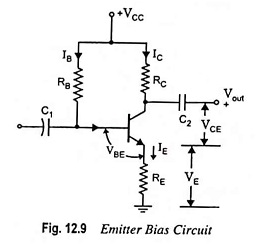
Emitter Bias Circuit Diagram:
This Emitter Bias Circuit Diagram is obtained by simply introducing an emitter resistor to the fixed bias circuit as shown in Fig. 12.9. For analysis, we will first examine the base-emitter loop and then use the results to investigate the collector-emitter loop.
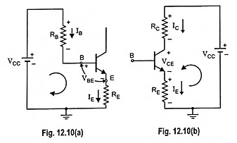
The base-emitter loop of the network given in Fig. 12.9 may be redrawn as shown in Fig. 12.10(a). Applying KVL around the indicated loop, we have
Note that the only difference between the above equation and equation for the fixed bias configuration
is the term (β + 1)RE.
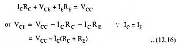
The collector-emitter loop is redrawn in Fig. 12.10(b).
Applying KVL for the indicated loop, we have
Voltage from emitter-to-ground is
![]()
while the voltage from collector-to-emitter is
![]()
Collector voltage,
![]()
and Base voltage,
![]()
![]()
From Eq. (12.15), we have
![]()
Differentiating above equation w.r.t. lC (considering VBE to be independent of lC), we have
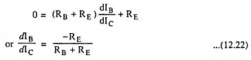
From Eq. (12.5) stability factor S is given as
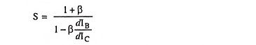
Substituting the value of dIB/dIC from Eq. (12.22) in above expression, we have
Stability factor,
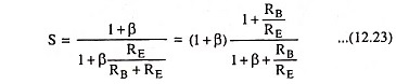
The above equation indicates that stability factor S varies between 1 for smaller values of RB/RE and (1 + β) for larger values of RB/RE. For proper operation both VCC and RE should be larger and RB smaller.
The addition of the emitter resistor to the dc bias of the BJT provides improved stability, i.e., the dc bias currents and voltages remain closer to where they were fixed by the circuit when the outside conditions, such as temperature, and transistor beta change.