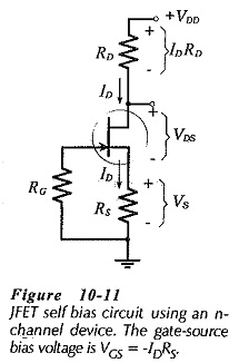
Self Bias Circuit Diagram:
Circuit Operation – In a self bias JFET circuit, gate-source bias is provided by the voltage drop across a resistor in series with the device source terminal. Consider the n-channel JFET Self Bias Circuit Diagram illustrated in Fig. 10-11. The voltage drop across resistor RS is,
![]()
If ID = 1 mA and RS = 1 kΩ, then VS =1 V. This means that, the source terminal in Fig. 10-11 is 1 V positive with respect to ground. Alternatively, ground can be said to be 1 V negative with respect to the source terminal. Because the FET gate terminal is grounded via RG (and there is no voltage drop across RG), the gate is 1 V negative with respect to the source. That is, the gate-source bias voltage is VGS = -1 V. So, for a Self Bias Circuit Diagram,
![]()
The fact that ID determines VGS, and that VGS sets the ID level, means that there is a feedback effect tending to control ID. Thus, if ID increases when the device is changed, the increased voltage across RS results in an increased (negative) gate-source voltage that tends to reduce ID back toward its original level. Similarly, a fall in ID produces a reduced VGS which tends to increase ID toward its original level.
Circuit Analysis:
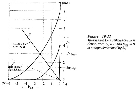
As for all FET bias circuits, a graphical technique is most convenient for analysis of a Self Bias Circuit Diagram. In this case, the bias line drawn on the transfer characteristics is quite different from that for the gate bias circuit. The value of RS and convenient ID levels are inserted into Eq. 10-4 to determine corresponding VGS levels. The ID and VGS values are plotted on the transfer characteristics, and the bias line is drawn through them, (see Fig 10-12). The intersection points of the bias line and the transfer characteristics gives the maximum and minimum ID levels.
Summing the voltage drops across RD, RS, and the FET drain-source terminals in Fig. 10-11 gives,
![]()
Equation 10-5 may be used to calculate the maximum and minimum levels of VDS when ID(max) and ID(min) have been determined.
Self-Bias for a p-channel JFET:
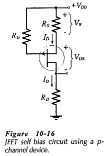
A Self Bias Circuit Diagram using a p-channel JFET is shown in Fig. 10-16. The gate-source bias voltage is once again provided by the voltage drop across source resistor RS. In this case, the source is negative with respect to the supply voltage (+VDD). Because the gate is connected to +VDD via RG, the gate is is positive with respect to the source terminal. The positive level of VGS provides the reverse bias at the gate-channel junctions of the p-channel FET. A p-channel Self Bias Circuit Diagram can be analyzed in exactly the same way as an n-channel circuit.