FET Biasing Methods – Fixed Bias, Self Bias, Potential Divider Bias and Current Source Bias:
Unlike BJTs, thermal runaway does not occur with FETs. However, the wide differences in maximum and minimum transfer characteristics make ID levels unpredictable with simple fixed-gate bias voltage. To obtain reasonable limits on quiescent drain currents ID and drain-source voltage VDS, source resistor and potential divider bias techniques must be used. With few exceptions, MOSFET bias circuits are similar to those used for JFETs. Various FET Biasing Methods are discussed below :
Fixed Bias:
In this FET Biasing Methods, DC bias of a FET device needs setting of gate-source voltage VGS to give desired drain current ID. For a JFET drain current is limited by the drain-source saturation current IDSS. Since the FET has such a high input impedance that no gate current flows and the dc voltage of the gate set by a voltage divider or a fixed battery voltage is not affected or loaded by the FET.
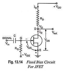
Fixed dc bias is obtained using a battery VGG. This battery ensures that the gate is always negative w.r.t. source and no current flows through resistor RG and gate terminal i.e. IG ≡ 0. The battery provides a voltage VGS to bias the N-channel JFET, but no resulting current is drawn from the battery VGG. Resistor RG is included to allow any ac signal applied through capacitor C to develop across RG. While any ac signal will develop across RG, the dc voltage drop across RG is equal to IGRG i.e. 0 volt.
The gate-source voltage VGS is then
![]()
The drain-source current ID is then fixed by the gate-source voltage.
This current then causes a voltage drop across the drain resistor RD and is given as
![]()
and output voltage,
![]()
Since VGG is fixed value of dc supply and the magnitude of gate-to-source voltage VGS is also fixed, hence this circuit is named as fixed bias circuit. Since this bias circuit uses two batteries VDD and VGG, it is also known as two battery bias circuit.
A FET has a high input impedance. To make advantage of it, RG should be as large as possible so that the input impedance of the circuit remains high. If RG is extremely large a charge accumulated on the gate may take a long time to leak off. A reasonable upper limit is 1 MΩ. Normally RG should not exceed this value.
Self-Bias:
This is the most common FET Biasing Methods. Self-bias for an N-channel JFET is shown in Fig. 13.15. This circuit eliminates the requirement of two dc supplies i.e., only drain supply is used and no gate supply is connected. In this circuit, a resistor RS, known as bias resistor, is connected in the source leg.
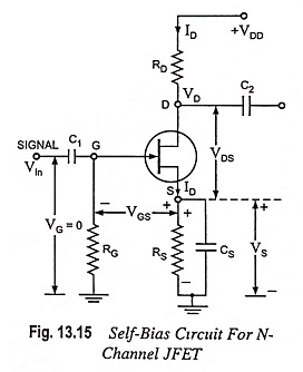
The dc component of drain current ID flowing through RS makes a voltage drop across resistor RS. The voltage drop across RS reduces the gate-to-source reverse voltage required for FET operation. The capacitor CS bypasses the ac component of the drain current ID. The addition of resistor RG in the circuit does not disturb the dc bias. This is because gate current flowing through it is zero and the gate leakage current is also almost zero.
Thus, gate is essentially at dc ground. The resistor RG is inserted in the circuit to avoid the short circuiting of the ac input voltage. Further, if there is a leakage, the resistor RG will provide to it an escape route. Otherwise, the leakage current would build up static charge (voltage) at the gate which could change the bias. The resistor RS, the feedback resistor, also helps in preventing any variation in FET drain current.
Since no gate current flows through the reverse-biased gate, the gate current IG = 0 and, therefore,
![]()
With a drain current ID the voltage at the S is
![]()
The gate-to-source voltage is then
![]()
So voltage drop across resistance RS provides the biasing voltage VGS and no external source is required for biasing and this is the reason that it is called self-biasing.
The operating point (i.e. zero signal ID and VDS) can easily be determined and equation given below :
![]()
Thus dc conditions of JFET amplifier are fully specified.
Self-biasing of a JFET stabilizes its quiescent operating point against any change in its parameters like transconductance. Let the given JFET be replaced by another JFET having the double conductance then drain current will also try to be double but since any increase in voltage drop across RS, therefore, gate-source voltage, VGS becomes more negative and thus increase in drain current is reduced.
Potential Divider Bias:
A slightly modified form of DC FET Biasing Methods is provided by the circuit shown in Fig. 13.16. The resistors RG1 and RG2 form a potential divider across drain supply VDD. The voltage V2 across RG2 provides the necessary bias. The additional gate resistor RG1 from gate to supply voltage facilitates in larger adjustment of the dc bias point and permits use of larger valued RS.
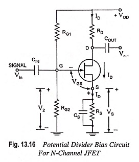
The gate is reverse biased so that IG = 0 and gate voltage
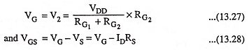
The circuit is so designed that IDRS is larger than VG (or V2) so that VGS is negative. This provides correct bias voltage.
The operating point can be determined as
Maximum gain is achieved by making resistance RD as large as possible and for a given level of ID it needs maximum voltage drop across resistor RD. However, greatest bias stability is achieved by making RS as large as possible.
If the gate voltage VG is very large as compared to gate-to-source voltage VGS, the drain current is approximately constant. In practice, the voltage divider bias is less effective with JFET than BJT. This is because in BJT, VBE = 0.7 V (silicon) with only minor variations from one transistor to another transistor. But in a JFET, the VGS can vary several volts from one JFET to another.
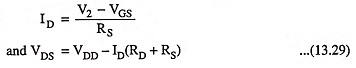
Current-Source Bias:
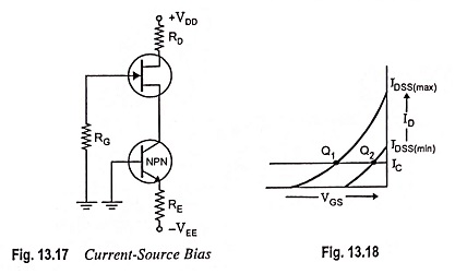
In this FET Biasing Methods, When the drain supply voltage VDD is not large, there may not be enough gate voltage to swamp out the variations in VGS. In such a case current-source bias (Fig. 13.17) may be used. In this arrangement, the BJT pumps a fixed current through the JFET. The drain current is given by
![]()
Figure 13.18 illustrates how effective current-source bias is. Both Q points have the same value of drain current. Although VGS is different for each Q point, VGS no longer has any effect on the value of drain current.