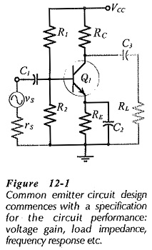
Single Stage Common Emitter Amplifier Circuit:
Specification – Bias circuit design for the Single Stage Common Emitter Amplifier Circuit in shown in Fig. 12-1 and ac analysis of the circuit is already explained. Design of this circuit (or any other circuit) normally commences with a specification which might list: the supply voltage, minimum voltage gain, frequency response, signal source impedance, and the load impedance.
Selection of IC, RC, and RE
Designing for a particular voltage gain requires the use of ac negative feedback to stabilize the gain. The circuit shown in Fig. 12-1 has no provision for negative feedback, consequently, it is designed to achieve the largest possible voltage gain. From Eq. 6-15, the voltage gain of a Single Stage Common Emitter Amplifier Circuit,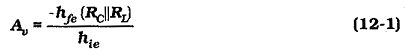
Because Av is directly proportional to RC||RL, design for the greatest voltage gain would seem to require selection of the largest possible collector resistance. However, a very large value of RC might make the collector current too small for satisfactory transistor operation. For most small-signal transistors, IC should not be less than 500 μA. A good minimum IC to aim for is 1 mA. Special low-noise transistors operate with much lower collector current levels.
The transistor hfe value is related to IC, so IC might be selected high to give the largest hfe, again to achieve the greatest Av. But, a high IC level results in a small RC value for a given voltage drop (VRC). So, a high IC level might actually result in a low Av value, although hfe might be relatively large.
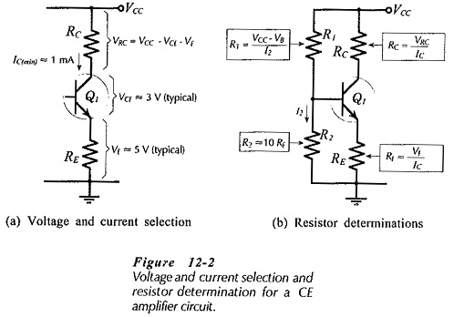
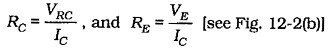
For a given level of IC, the largest possible voltage drop across RC gives the greatest RC value, (RC = VRC/IC). To make VRC as large as possible, VCE and VE should be held to a minimum, [see Fig. 12-2(a)]. The collector-emitter voltage should typically be around 3 V. This is large enough to ensure that the transistor operates linearly, and it also allows for a collector voltage swing of ±1 V which is usually adequate for a small-signal amplifier. Another consideration in selecting RC is that there is nothing to be gained by making RC larger than RL. In fact, RC should normally be very much smaller than RL, so that RL has little effect on the circuit voltage gain.
For good bias stability, the emitter resistor voltage drop (VE) should be much larger than the base-emitter voltage (VBE). This is because VE = VB – VBE, and when VE ≫ VBE, VE will be only slightly affected by any variation in VBE (due to temperature change or other effects). Consequently, IE and IC remain fairly stable at IC ≈ IE = VE/RE. A minimum VE of 5 V gives good bias stability in most circumstances, [see Fig. 12-2 (a)]. With supply voltages less than 10 V, VE might have to be reduced to 3 V to allow for reasonable levels of VCE and VRC. Normally, an emitter resistor voltage drop less than 3 V is likely to produce poor bias stability.
Once VE, VCE, and IC are selected, VRC is determined as,
![]()
Then, RC and RE are calculated,
Bias Resistors:
As we know already, selection of the voltage divider current (I2) as IC/10 gives good bias stability and reasonably high input resistance. Where the input resistance is not important, I2 may be made equal to IC for excellent bias stability. The bias resistors are calculated as,
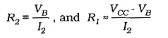
Selecting R2 = 10 RE gives I2 ≈ IC/10, [Fig. 12-2(b)]. The precise level of I2 can be calculated as I2 =VB/R2, and this can be used in the equation for R1.
Bypass Capacitor:
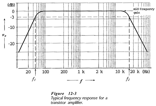
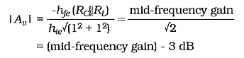
All capacitors should be selected to have the smallest possible capacitance value, both to minimize the physical size of the circuit and for economy (large capacitors are the most expensive). Because each capacitor has its highest impedance at the lowest operating frequency, the capacitor values are calculated at the lowest signal frequency that the circuit is required to amplify. This frequency is the circuit lower cutoff frequency, or low 3 dB frequency (f1), (see Fig. 12-3).
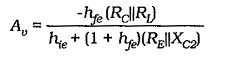
Bypass capacitor C2 in Fig. 12-1 is normally the largest capacitor in the circuit, so C2 is selected to set f1 at the desired frequency. Voltage gain was developed for a Single Stage Common Emitter Amplifier Circuit with an unbypassed emitter resistor (RE). Rewriting the equation to include XC2 in parallel with RE gives
Normally RE ≫ XC2, so RE can be omitted. Also, XC2 is capacitive,
so,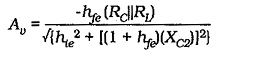
when hfe = (1 + hfe) XC2,
Therefore, at f1,
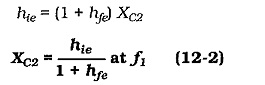
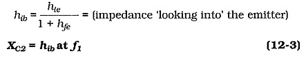
At f1,
![]()
Equations 12-2 and 12-3 give the smallest value for the bypass capacitor. When selecting a standard value for the capacitor, the next larger value should be chosen. This will give a cutoff frequency slightly lower than the f1 value used in the calculations.
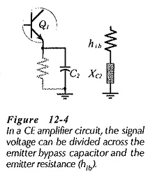
It is important to note that the emitter bypass capacitor is calculated in terms of the resistance ‘seen looking into’ the transistor emitter terminal (the resistance in series with C2). The capacitor value is not determined in relation to the value of the emitter resistor (RE).
Coupling Capacitors:
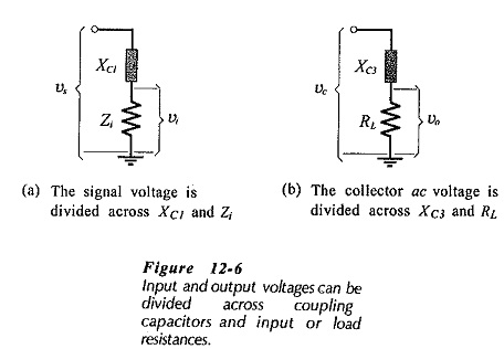
The coupling capacitors (C1 and C3 in Fig. 12-1) should have a negligible effect on the frequency response of the circuit. Figure 12-6(a) illustrates the fact that XC1 and Zi constitute a voltage divider If XC1 is too large, the circuit ac input voltage (vi) will be significantly smaller than the signal voltage (vs). Similarly, XC3 and RL attenuate the ac voltage at the transistor collector, so that the ac output voltage (vo) can be smaller than the ac collector voltage (vo), [Fig. 12-6(b)]. To minimize the effects of C1 and C3, the reactance of each coupling capacitor is selected to be approximately equal to one-tenth of the impedance in series with it at the lowest operating frequency for the circuit (f1).
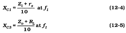
Usually, RL ≫ Zo, and often Zi ≫ rs, so that Zo and rs can be omitted in Equations 12-4 and 12-5. Once again, the equations give minimum capacitance values, so that the next larger standard values should always be selected for C1 and C3.
Equations 12-4 and 12-5 give an impression that approximately 10% of the signal and output voltages are lost across C1 and C3. This would be true if the quantities were resistive. However, XC1 and XC3 are capacitive while Zi and RL are usually resistive. So, when the actual loss is calculated, it is found to be only around 0.5% for each capacitor.
Another approach to the selection of coupling capacitors is to make XC1 = Zi at two octaves below f1.
![]()
The output coupling capacitor is then determined by making impedance of C3 equal to RL at two octaves below f1/4.
![]()
When Equations 12-6 and 12-7 are used to determine the values of the coupling capacitors, it can be shown that the capacitor attenuation effects are less than 5% of Av.
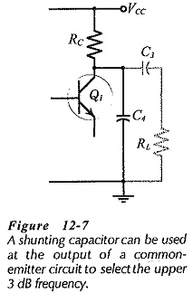
Shunting Capacitor:
Sometimes an amplifier is required to have a particular upper cutoff frequency, (f2 in Fig. 12-3). The transistor must be selected to have a much higher cutoff frequency than f2. The upper cutoff frequency for the circuit can then be set by connecting a small capacitor from the transistor collector terminal to ground, (C4 in Fig. 12-7).