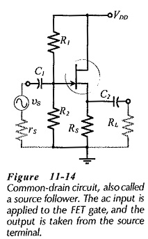
Common Drain Amplifier Circuit Diagram:
The FET Common Drain Amplifier Circuit Diagram shown in Fig. 11-14 has the output voltage developed across the source resistor (RS). The external load (RL) is capacitor-coupled to the source terminal of the FET, and the gate bias voltage (VG) is derived from VDD by means of voltage divider resistors R1 and R2. No resistor is connected in series with the drain terminal, and no source bypass capacitor is employed.
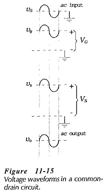
To understand the operation of the circuit in Fig. 11-14 note that the dc gate voltage (VG) is a constant quantity, and the source voltage is,
![]()
When an ac signal is applied to the gate via capacitor C1, the gate voltage is increased and decreased as the instantaneous level of the signal voltage rises and falls. Also, VGS remains substantially constant, so the source voltage increases and decreases with the gate voltage. (See the wave forms in Fig. 11-15.) Thus, the ac output voltage is closely equal to the ac input voltage, and the circuit can be said to have unity gain. AC analysis of the circuit shows that vo is slightly smaller than vi. Because the output voltage at the source terminal follows the signal voltage at the gate, the Common Drain Amplifier Circuit Diagram is also known as a source follower.
Common Drain Equivalent Circuit:
As in the case of other circuits, the supply voltage and coupling capacitors in Fig. 11-14 must be replaced with short-circuits in order to study the circuit ac performance. This gives the common-drain ac equivalent circuit in Fig. 11-16(a). The input terminals of the ac equivalent circuit are seen to be the FET gate and drain, and the output terminals are the source and drain. Because the drain terminal is common to both input and output, the circuit configuration is named common-drain (CD).
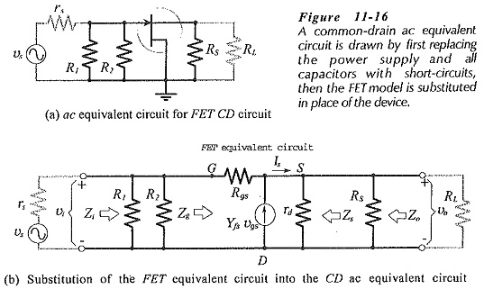
The completer CD ac equivalent circuit is drawn by substituting the FET model into the ac equivalent circuit, rig. 11-16(b)]. The indicated current directions and voltage polarities are, once again, those that are produced by a positive-going signal voltage.
Input Impedance:
Looking into the gate and drain terminals in Fig. 11-16(b), is similar to looking into the input of a common-source amplifier with an unbypassed source resistor. Therefore, the common-drain Zg equation is derived in the same way as we know already. One important difference is that the Common Drain Amplifier Circuit Diagram has the external load resistor (RL) in parallel with RS.
![]()
As discussed already, the equation for Zg gives a very large value. This is important only when the signal source is connected directly in series with the gate terminal. With the signal capacitor-coupled to the input, the circuit input impedance is,
![]()
which reduces to,
![]()
Output Impedance:
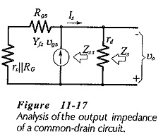
In a Common Drain Amplifier Circuit Diagram, any variation in the output voltage (vo) has an effect on the FET gate-source voltage. To determine the impedance looking into the source terminal, the signal voltage [in Fig. 11-16(b)] is assumed to be zero, and the output current (Is) is calculated in terms of vo. The circuit is redrawn in Fig. 11-17 with resistor RG representing the gate bias resistors, [RG = R1||R2 in Fig. 11-16(a)]. With vs = 0, vo is divided across RG||rs and Rgs, (see Fig. 11-17). Because Rgs ≫ (RG||rs), effectively all of vo is applied as an ac gate-source voltage. So,
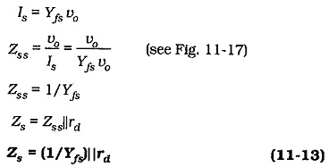
Equation 11-13 gives the device output impedance. The circuit output impedance also involves RS.
![]()
The drain resistance is usually much larger than RS, and Rs is usually much larger than 1/Yfs, so that Zo ≈ 1/Yfs. For Yfs = 5000 μS, Zo = 200 Ω.
Voltage Gain:
From Fig. 11-16(b),
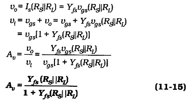
As already discussed, the ac output voltage from a CD circuit is usually closely equal to the input voltage, so the voltage gain is normally taken as,
![]()
Summary of CD Circuit Performance:
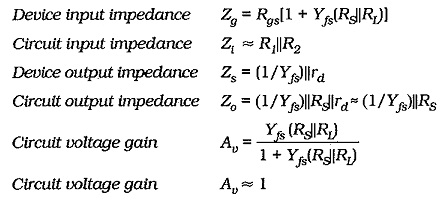
A Common Drain Amplifier Circuit Diagram has a voltage gain approximately equal to 1, no phase shift between input and output, very high input impedance, and low output impedance. Because of its high Zi, low Zo, and unity gain, the CD circuit is usually used as a buffer amplifier between a high impedance signal source and a low impedance load.