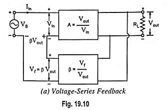
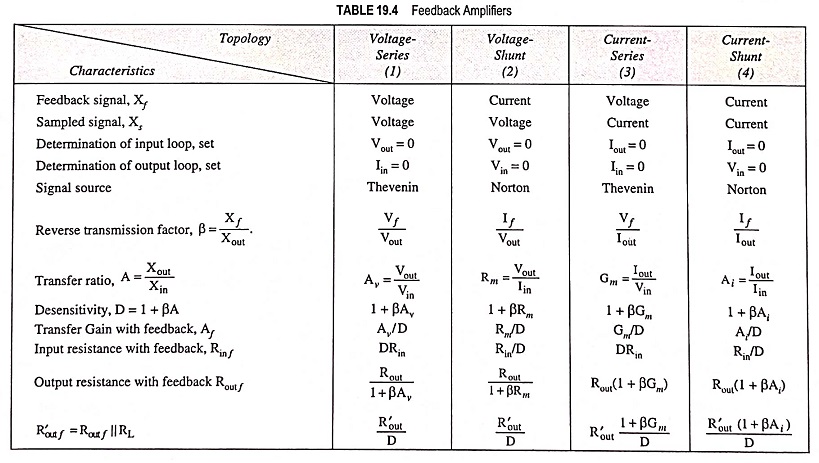
Voltage Series Feedback Amplifier or Shunt Derived Series Fed Feedback Amplifier:
Voltage Series Feedback Amplifier Circuit is also called the shunt-derived series-fed feedback. Here the amplifier and feedback network are connected in series-parallel. A fraction of the output voltage is applied in series opposition to the input voltage through feedback network, as shown in Fig. 19.10 (a).
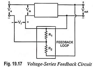
In a block diagram of Voltage Series Feedback Amplifier Circuit given in Fig. 19.17, the feedback voltage is derived from the voltage divider circuit formed of resistors R1 and R2. Thus feedback voltage is given as
![]()
Thus

As seen, the input impedance of the amplifier and output impedance of the feedback network appear in series to the input and therefore input impedance to the amplifier is increased by a factor (1 + βA).
Similarly input to the feedback network and output of the amplifier appear in parallel to the amplifier output. Thus, so far as Vout is concerned, output impedance of the amplifier is reduced, due to the shunting effect of the input to the feedback, by a factor 1/1 + βA.
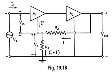
A general two stage amplifier having stage gains of A1 and A2 respectively is shown in Fig. 19.18. The output of the second stage is fed back through the feedback network R1R2 in opposition to the input signal voltage Vs. Obviously this circuit is a case of voltage-series negative feedback. It is expected that input impedance will increase, output impedance will decrease and voltage gain will be stabilized.
An approximate analysis can be made if the open-loop gain is assumed to be very large and I′ << 1. Under such conditions, we have
Vin ≈ 0 for a finite Vout, and
Supply voltage,

Thus
![]()
and overall gain with feedback,
From the above equation it is obvious that under the above conditions the voltage gain is independent of all parameters except R1 and R2. Thus, if these resistors are stable, the circuit amplification is stabilized.
Now let us consider FET common drain amplifier (source follower) and BJT common-collector amplifier (emitter follower) as examples of the voltage-series topology.
FET Source Follower :
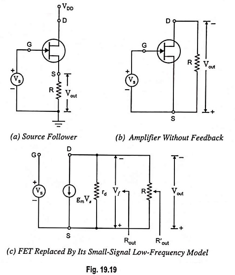
The circuit is shown in Fig. 19.19(a). In this circuit, no resistor is connected in series with the drain terminal and no source bypass capacitor is used. The input signal is applied to the gate G. The output voltage is developed across source resistor R. Sampled signal is the output voltage Vout across source resistor R and feedback signal is the voltage Vf across R. Thus, it is the case of Voltage Series Feedback Amplifier Circuit and reference should be made to the first topology in Table 19.4.
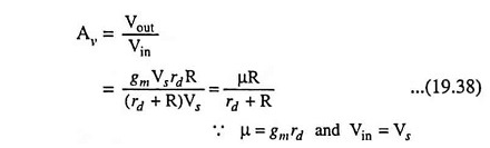
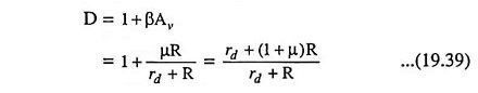
For drawing basic amplifier without feedback, input circuit is obtained by setting Vout = 0 and output circuit is obtained by setting Iin = 0. Thus, Vs appears directly between G and S and R appears only in the output loop, as shown in Fig. 19.19 (b). Figure 19.19 (b) represents the amplifier circuit without feedback. Replacing FET by its small signal low-frequency model, we have the circuit as shown in Fig. 19.19 (c).
From the circuit shown in Fig. 19.19 (c).
Output voltage Vout and feedback voltage Vf are equal, so
Reverse transmission factor, β = Vf/Vout = 1
The topology stabilizes the voltage gain.
Input voltage without feedback, Vin = Vs [Refer to Fig. 19.19 (b)]
From Fig. 19.19 (c)
Voltage gain,
Desensitivity,
and voltage gain with feedback,

The input impedance of an FET is infinite, Rin = ∞, and therefore,
![]()
We are interested in determination of output resistance looking into the FET source S. Hence R is considered as an external load resistance RL.
The output resistance,
Refer to first column of Table 19.4
BJT Emitter Follower:
The circuit is depicted in Fig. 19.20(a). In this circuit no emitter bypass capacitor is used. The feedback signal is the voltage Vf across emitter resistor Re and the sampled signal Vs is the output voltage across emitter resistor Re. Thus, it is a case of Voltage Series Feedback Amplifier Circuit and first topology in Table 19.4 should be referred.
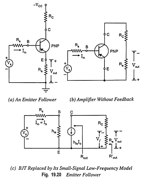
For drawing basic amplifier without feedback, input circuit is obtained by setting Vout = 0 and output circuit is obtained by setting Iin = Ib = 0. Thus, Vs in series with Rs appears between B and E and Re appears only in the output loop, as depicted in Fig. 19.20 (b). Fig. 19.20 (b) represents the amplifier circuit without feedback. Replacing BJT by its small-signal low-frequency model, we have circuit as shown in Fig. 19.20 (c).
From the circuit shown in Fig. 19.20 (c)

This topology stabilizes the voltage gain.
From inspection of Fig. 19.20 (c)
Voltage gain,
Desensitivity,
Voltage gain with feedback,
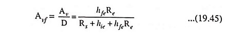
For hfeRe >> (Rs + hie), Avf ≈ 1, as it is expected for an emitter follower.
The input resistance without feedback,
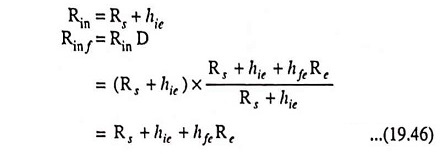
We are interested in determination of resistance seen looking into the emitter. So Re is considered as an external load. From Table 19.4
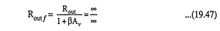
Because from Fig. 19.20 (c), we are looking into a current source,

The indeterminacy in Eq. (19.47) may be resolved by first evaluating R′out f and then going to the limit Re → ∞. Thus, since R′out = Re,
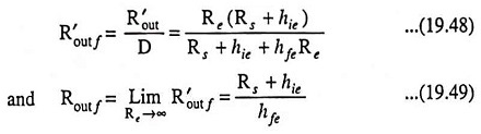
Note that the feedback desensitizes voltage gain with respect to variations in hfe and that it increases the input resistance and reduces the output resistance.
The foregoing expressions for Avf, Rin f and Rout f are based on the assumptions that there is zero forward transmission through the feedback network. But it is not true. On contrary there is such forward transmission due to flow of input current through Re in Fig. 19.20 (a) and so these expressions are only approximately true. Here we have in effect neglected the base current that flows in Re compared with the collector current.